I'll try that this weekend...
So how did the temperature/imbalance stability tests work out?
I had a closer look at my simulations of the Bob Cordell resistor fix to the balance problem.
I was concerned because it seems a blunt instrument, reduces sensitivity to the imbalance only as it reduces the gain.
But a closer look shows that, while this is true at DC and low frequencies, once you include the compensation then it is the compensation that dominates in the difficult hi-frequency area.
So the simple fix is pretty effective, as expected for Bob's work.
As usual, more subtleties and trade-offs than are obvious.
Best wishes
David
Hi David, the result was disappointing. The circuit works well when transistors are matched, however Hfe mismatching by 20% in one of the IPS pairs resulted DC offset at output, VAS bias current went up and down depending which of the transistors in the LTP has higher Hfe, the OPS bias current went up/down in turn, and THD suffered as well. These also drift along with temperature rise. I did not go deeper than the above, instead dug the forum and found threads about this topic. There did not seem to be a good solution that functions well yet maintain a simplicity in construction.
The topology itself has an appealing appearance yet the real world implementation can be frustrating as the merits from this complementary construction seem to rely on tight device matching.
The push-pull VAS transistors must have equal bias current, and this is achieved by the feedback mechanism with the complementary diff-pairs fighting each other by throwing the DC level at output off zero and by sacrificing a constant value of the common bias current going through the push-pull VAS transistors, when there is mismatching in transistor pairs.
I've largely decided to abandon the full complementary topology for the project and come back to "normal" VFS design. I think I owe you a big thank-you for sounding the alarm.
...The circuit works well when transistors are matched, however... found threads about this topic...not a... solution that functions well yet maintain a simplicity in construction.
Yes, it looks so attractive BUT!😉
A CommonModeControlLoop can be implemented with only 2 extra transistors, 4 is better for temperature stability but that's still not too bad.
Did you look at Edmond Stuart's "SuperTIS"? A fresh approach with new ideas.
That has no current gain in the TIS/"VAS" so imbalance in the IPS is not amplified.
An intermediate possibility between that and your Beta enhanced VAS would be a cascoded VAS.
I suspect that would be practicable with well matched IPS transistors that were thermally coupled via a shared heat-sink, in a shield box too would be even better.
Best wishes
David
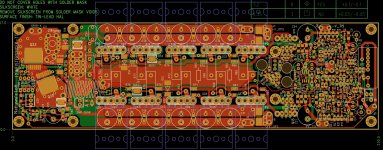
I Built This Thing, and it Works!
1.5 years have slipped by since this thread started and I’m glad I did not give up on the IPS and actually built the amp. Fired up power the last few days and it seems to be a success! 🙂
There has been a few changes to the original schematic in order to address the probable VAS current stability/sensitivity issue, and I believe they have worked in tandem and yielded a good result.
1) Matched dual transistors are used for the input pairs and current mirrors,
2) EF-enhanced VAS was replaced with Cascoded VAS for a much lower current gain – predictably less sensitivity on the VAS standing current – much thanks to Dave Zan.
3) a CFP bias spreader that has immunity to the VAS current variation, and ability to trim the bias without affecting the compensation tempco at the same time.
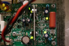
I did not screen and sort any of the small signal transistors, diodes, LEDs, all straight out of tube/tape then on the PCB, including all TO-126s and TO-220s. On-Semi ThermalTrak power transistors have quite good consistence in Vbe and Hfe. I have one tube of 25pcs NJL3281 and one tube of 25pcs NJL1302, and it was very easy to make groups of 5 having Vbe within 1mV and Hfe within 10%. I did not match Vbe and Hfe between genders.
IPS tail currents are almost exactly as the LTSpice has anticipated, and the VAS idle current was 1mA lower than simulation, consistently on both channels. The VAS degeneration resistors have since been reduced from 133-R to 113-R to get the VAS current back to 6mA.
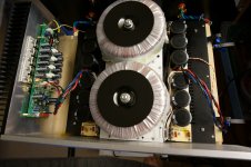
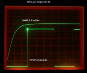
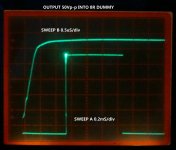
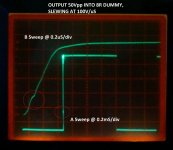
The output stage seems to have excellent bias control stability and accuracy. A test I repeated a few times gave the same results that I’m quite happy with. It started with the heat sink idling at stable 43C with 44mV between NPN-PNP emitters over two 0.33-R emitter resistors (67mA per pair), then I had the amp put out a 50Vp-p square wave into an 8-R dummy load, bringing the heat sink to a good hot 60C after quite a while, then removed the signal, the bias voltage would snaps back instantly to 43.8mV and stayed there.
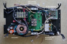
Other circuit around the amp, the DC servo, the solid state speaker relays, the soft starter, the OPS rail monitor, and the reservoir cap discharger, all worked as intended. The over-current protection will trip and latch the speaker relay out when it sees 1.65V over the 0.33R resistor, it was tested working in a static forced test, but I’m not ready to test it in a real over-current condition with the amp.
I'll have some pictures about the build and square wave signal tests coming up soon.
1.5 years have slipped by since this thread started and I’m glad I did not give up on the IPS and actually built the amp. Fired up power the last few days and it seems to be a success! 🙂
There has been a few changes to the original schematic in order to address the probable VAS current stability/sensitivity issue, and I believe they have worked in tandem and yielded a good result.
1) Matched dual transistors are used for the input pairs and current mirrors,
2) EF-enhanced VAS was replaced with Cascoded VAS for a much lower current gain – predictably less sensitivity on the VAS standing current – much thanks to Dave Zan.
3) a CFP bias spreader that has immunity to the VAS current variation, and ability to trim the bias without affecting the compensation tempco at the same time.
I did not screen and sort any of the small signal transistors, diodes, LEDs, all straight out of tube/tape then on the PCB, including all TO-126s and TO-220s. On-Semi ThermalTrak power transistors have quite good consistence in Vbe and Hfe. I have one tube of 25pcs NJL3281 and one tube of 25pcs NJL1302, and it was very easy to make groups of 5 having Vbe within 1mV and Hfe within 10%. I did not match Vbe and Hfe between genders.
IPS tail currents are almost exactly as the LTSpice has anticipated, and the VAS idle current was 1mA lower than simulation, consistently on both channels. The VAS degeneration resistors have since been reduced from 133-R to 113-R to get the VAS current back to 6mA.
The output stage seems to have excellent bias control stability and accuracy. A test I repeated a few times gave the same results that I’m quite happy with. It started with the heat sink idling at stable 43C with 44mV between NPN-PNP emitters over two 0.33-R emitter resistors (67mA per pair), then I had the amp put out a 50Vp-p square wave into an 8-R dummy load, bringing the heat sink to a good hot 60C after quite a while, then removed the signal, the bias voltage would snaps back instantly to 43.8mV and stayed there.
Other circuit around the amp, the DC servo, the solid state speaker relays, the soft starter, the OPS rail monitor, and the reservoir cap discharger, all worked as intended. The over-current protection will trip and latch the speaker relay out when it sees 1.65V over the 0.33R resistor, it was tested working in a static forced test, but I’m not ready to test it in a real over-current condition with the amp.
I'll have some pictures about the build and square wave signal tests coming up soon.
Attachments
Last edited:
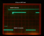
Responds to Square Wave - no slew-overdrive
I don't have a function generator and have been using a home brew 2.5Vp-p square wave oscillator that is capable of steep transition edges that are well under 10nS. With the 1k1-220pF input LPF in place the amp is able to follow nicely.
I don't have a function generator and have been using a home brew 2.5Vp-p square wave oscillator that is capable of steep transition edges that are well under 10nS. With the 1k1-220pF input LPF in place the amp is able to follow nicely.
Attachments

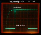
Responds to Square Wave - Slew Overdriven
The input LPF was relaxed by reducing the 220pf shunt cap to 47pF, just trying to see how the amp behaves when slew-overdriven. The output slewed at a rate of slightly over 100V/uS. The wrinkle on the lower part of the rising edge indicates the moment the feedback loop loses control of the amp.
I think this amps performs quite nicely from its square wave response.
The next I'll have to build/buy some sine generator and perhaps distortion meter/analyzer for more tests.
Attachments
....in order to address the probable VAS current stability/sensitivity issue, and I believe they have worked in tandem...
1) Matched dual transistors are used for the input pairs and current mirrors,
2) EF-enhanced VAS was replaced with Cascoded VAS for a much lower current gain... much thanks to Dave Zan...
Very happy to see that this worked out for you, and to have been able to help.
Always a pleasure when the theory checks out in reality.😉
Looks like a very nice build, my compliments to your exemplary work.
Best wishes
David
Last edited:
You can find a capacitor in place of C29 in every amp that uses a Vbe multiplier to generate bias voltage for OPS. It's function is to help keeping both sides of the Vbe multiplier at the same AC potential at very high frequencies where the Vbe multiplier can have an elevated impedance. This cap usually has no impact on stability of the amp.
C30 was optional and was later removed from the final layout design to make room for the improved bias voltage circuit. This cap can help speed up purging the base region of the output transistor at turning off. I have since decided to permanently use a two ThermalTrak diode string to load the driver transistors to keep the impedance between the output transistors' base low, C30 was then no long needed.
C30 was optional and was later removed from the final layout design to make room for the improved bias voltage circuit. This cap can help speed up purging the base region of the output transistor at turning off. I have since decided to permanently use a two ThermalTrak diode string to load the driver transistors to keep the impedance between the output transistors' base low, C30 was then no long needed.
I am not sure we are talking about the same caps.
I took the position numbers based on your very first post and schematic.
The 1nF || on the VAS emitter resistors on both +/- side.
BTW: could you share this very fast step up signal generator circuit as well?
I took the position numbers based on your very first post and schematic.
The 1nF || on the VAS emitter resistors on both +/- side.
BTW: could you share this very fast step up signal generator circuit as well?
Ah, I see. That circuit was never built. And c29/30 became c13/14 in the final circuit posted in #24. These caps alter the output impedance of VAS at high frequencies and help taming the peaking in the frequency response of the 3EF OPS. They improve the gain margin slightly in the loop gain plot.
The square wave generator is a simple one like this, I buffered the output of the oscillator with the other 5 gates in the 74HC14 paralleled together. The power regulator is a TL431 that puts out 2.5v. If you have an old function generator that you want to sharpen up the edges of its square you can buffer it with a 74HC14 using all its 6 gates paralleled together.
The square wave generator is a simple one like this, I buffered the output of the oscillator with the other 5 gates in the 74HC14 paralleled together. The power regulator is a TL431 that puts out 2.5v. If you have an old function generator that you want to sharpen up the edges of its square you can buffer it with a 74HC14 using all its 6 gates paralleled together.
Yes, C13/14 values are from simulation. I try not to over-do it by using small value ones, so I backed off from 1000pF to 470pF and with a 22-R resistor in series.
220-R resistor at each gate isn't really necessary, the gates within a package are closely matched enough to not to have troubles when directly connected together. I do have a 47-R at the combined output.
220-R resistor at each gate isn't really necessary, the gates within a package are closely matched enough to not to have troubles when directly connected together. I do have a 47-R at the combined output.
- Status
- Not open for further replies.
- Home
- Amplifiers
- Solid State
- Meistersinger VFA-200, A beginner’s first try in LTSpice