Some time ago, I was doing a design for an MM with no feedback,
using a one-stage transconductance. That worked just fine, so I
wanted to do the same for an MC pre-amplifier.
The problem is that all the design I've seen, (on MC head amps),
uses on or more large electrolytics, and I definitely wanted to
avoid that, so the challenge was to make an amplifier with
these basic features:
1)a gain of 80dB @ dc,
2)an input bias-current < 1muA
3)low noise
4)using easy to obtain components
The concept I was working from is as simple as it gets:

The dc-gain is defined as Ag = gm x Rl and with Rl = 33k5 in
the RIAA network and Ag = 80dB = 10,000x =>
gm = 10k/33k5 =0.298S (S = 1/Ohm).
The RIAA network is from Linsley-Hood as found on Elliot Sound
(sound-au.com/project25.htm), allthough I reduced the impedance-
level to 1/3, i.e. resistors devided by 3 and capacitors multiplied
be 3.
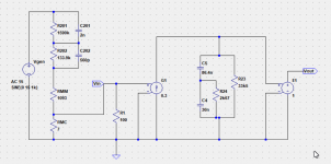
The design I came up with look like this (simplified):

The output of the LTPs (Long Tailed Pair) feeds into a combination
of a current mirror and folded cascode. With the R4,R5, and R6 as
specified, the quiscent currents of Q9, Q12 and Q6 are the same.
The same applies for Q1, Q4, and Q14.
The total gm from input to the RIAA network is :
gm = a x b c x Ic/Vt,
where
a = ½ as the input voltage is shared between each transistor
in the LTP,
b = 2 as there is two LTPs,
c = 3 well its just way the current mirror / folded cascode works,
Ic = the collector current in the LTPs, and
Vt = 26mV
Now we can calculate the Ic in the LTPs:
Ic = gm x Vt/3 = 0.298 x 26mV/3 = 2.58mA, and hence
R3 = R7 = (15-0.7)/(2Ic) = 2.77kOhm
Now, if you simulate (or build) the amp, the gain at LF/DC just can't
make it to 80dB. The problem is the Q6 and Q14 : the output impedance
is too low. This is dealt with in the full design.
A few words on the output buffer: The requirements of this buffer are:
1) A high input impedance, as not to load the RIAA network
2) Drive the output (!)
3) Low distortion.
1) states that Q17 and Q18 should run at a rather low Ic,
2) states that Q19 - Q22 should run at a "not too low" current.
3) The original diamond buffer had only four transistors, and
run at the same Ic, as this cancels out much distortion, albeit at
a rather high total current.
By adding two transistors, the output transistors can be run at almost
the same current as the input transistors, and still be able to drive
any "normal" amplifier down the line. Running at 560muA each this buffer
will drive a 5.8kOhm load to 13V and still stay in class A. It will
drive much lower load, but then in class B. It should be able to drive
a 825 Ohm load to 13V.
There is another issue: the ouput offset voltage. In the simplified
version, LTSpice calculates it to be app 1V. But this is with
identical transistors, and with physical transistors this isbound to
be much larger. After all, the DC gain is 10,000x so just a 1mv
difference in the input transistors, this will result in 10V at
output! This is dealt with in the full circuit.
The full circuit will follow in a subsequent post
Have a nice day!
using a one-stage transconductance. That worked just fine, so I
wanted to do the same for an MC pre-amplifier.
The problem is that all the design I've seen, (on MC head amps),
uses on or more large electrolytics, and I definitely wanted to
avoid that, so the challenge was to make an amplifier with
these basic features:
1)a gain of 80dB @ dc,
2)an input bias-current < 1muA
3)low noise
4)using easy to obtain components
The concept I was working from is as simple as it gets:
The dc-gain is defined as Ag = gm x Rl and with Rl = 33k5 in
the RIAA network and Ag = 80dB = 10,000x =>
gm = 10k/33k5 =0.298S (S = 1/Ohm).
The RIAA network is from Linsley-Hood as found on Elliot Sound
(sound-au.com/project25.htm), allthough I reduced the impedance-
level to 1/3, i.e. resistors devided by 3 and capacitors multiplied
be 3.
The design I came up with look like this (simplified):
The output of the LTPs (Long Tailed Pair) feeds into a combination
of a current mirror and folded cascode. With the R4,R5, and R6 as
specified, the quiscent currents of Q9, Q12 and Q6 are the same.
The same applies for Q1, Q4, and Q14.
The total gm from input to the RIAA network is :
gm = a x b c x Ic/Vt,
where
a = ½ as the input voltage is shared between each transistor
in the LTP,
b = 2 as there is two LTPs,
c = 3 well its just way the current mirror / folded cascode works,
Ic = the collector current in the LTPs, and
Vt = 26mV
Now we can calculate the Ic in the LTPs:
Ic = gm x Vt/3 = 0.298 x 26mV/3 = 2.58mA, and hence
R3 = R7 = (15-0.7)/(2Ic) = 2.77kOhm
Now, if you simulate (or build) the amp, the gain at LF/DC just can't
make it to 80dB. The problem is the Q6 and Q14 : the output impedance
is too low. This is dealt with in the full design.
A few words on the output buffer: The requirements of this buffer are:
1) A high input impedance, as not to load the RIAA network
2) Drive the output (!)
3) Low distortion.
1) states that Q17 and Q18 should run at a rather low Ic,
2) states that Q19 - Q22 should run at a "not too low" current.
3) The original diamond buffer had only four transistors, and
run at the same Ic, as this cancels out much distortion, albeit at
a rather high total current.
By adding two transistors, the output transistors can be run at almost
the same current as the input transistors, and still be able to drive
any "normal" amplifier down the line. Running at 560muA each this buffer
will drive a 5.8kOhm load to 13V and still stay in class A. It will
drive much lower load, but then in class B. It should be able to drive
a 825 Ohm load to 13V.
There is another issue: the ouput offset voltage. In the simplified
version, LTSpice calculates it to be app 1V. But this is with
identical transistors, and with physical transistors this isbound to
be much larger. After all, the DC gain is 10,000x so just a 1mv
difference in the input transistors, this will result in 10V at
output! This is dealt with in the full circuit.
The full circuit will follow in a subsequent post
Have a nice day!
Attachments
Last edited:
I added two cascodes between Q6 and Q14 to increase the impedance, thereby decreasing the Riaa deviation.
I didn't have the BC transistors that you used in my library, so I replaced them all by 2N3904/2N3906 except for the input resistors, where I used very low noise the ZTX851/ZTX951.
To get the output nulled, I used a servo connected between output and cascode.
Noise is below 0,5 nV/rtHz or 71nV for the audio range from 20Hz to 20Khz.
Hope this helps you.
Hans

View attachment MC 5 mk III.asc
I didn't have the BC transistors that you used in my library, so I replaced them all by 2N3904/2N3906 except for the input resistors, where I used very low noise the ZTX851/ZTX951.
To get the output nulled, I used a servo connected between output and cascode.
Noise is below 0,5 nV/rtHz or 71nV for the audio range from 20Hz to 20Khz.
Hope this helps you.
Hans
View attachment MC 5 mk III.asc
Last edited:
Why this odd R5-R6 and R10-R11 dubble 300E in parallel instead on one 150E resistor?
I'm curous about the noise figures.
I'm curous about the noise figures.
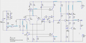
You beat me to it, Hans. But here is the full circuit as promised,
pls see attachment.
A lot has been added, relative to the simplified circuit. From left, I
have added 2 LTP in parrallel with the original, purely from noise
requirement. The reason for the BC639/BC640 is that a) it's readily
available and b) rumour has it, that they are merely BD139/140 in a
TO92 housing. In other words, medium power transistor, with a larger
chip compared to a normal small-signal one. I tried with 2sa1316 and
2sc3329 - they are specified as input transistors for MC amps, but
they sim worse - for what its worth - than BC639/BC640. The reason for
parelleling LTPs in stead of transistors is a practical on: it is much
easier to find 2 pairs than finding 4 transistors that match within,
say, 1mV from a batch of say 20 transistors.
MarsBravo: regarding R5/6 and R9/10, you are absolutely right. The
reason is that I some time ago bought 1000 pcs of 300 Ohms 1% for
next to nothing.
The next addition are Q7/8 (and Q15/16). Instead of a cascode, I
chose to use boot-strapping. There are two reasons for this.
Firstly, it is superior to the cascoding, as it maintains a constant
voltage over the boot-strapped transistor, Q6 an Q14. Secondly, the base
current flowing into Q7 cancels out the base current flowing out of
Q6, thereby improving the performance of the current mirror. R19 is
added to improve in this regard.
With a gain at LF/DC of 80dB, the output offset would be huge, even
with matched transistors. Even though I wanted to avoid using ICs,
I had to capitulate. I have not been able to come up with a simple
design for a servo. So hence the 2 OP-amps. The OP-amp here is LT1057,
but you could use OPA2134 or maybe even TL072. There is no reason to
use a very high spec (=expensive) OP-amp.
In stead of messing with the input transistors, I chose the approch
that you would find in OP-amps. Note the net labels BPA(Bias Positive A),
BPB(Bias Positive B), BNA (Bias Negative A), BNA (Bias Negative B),
which are also found in the current mirrors. Notice the output voltage
of the OP-amps: 2.2V and -2.2V respectively. In a real build, it might
be neccesary to reduce R30-R32.
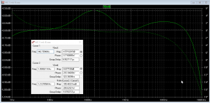
Simulation results:
I've attached an AC plot of the RIAA accuracy : in short it's within
0.1dB from app 3Hz to 37kHz.
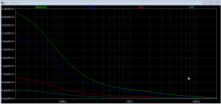
You'll also find a noise-plot which shows, that the primary noise
source is the MC-resistance (blue trace), #2 is the input-
transistors - there are 8, and I've only included one (red trace),
and #3 are the emitter resistors of the current mirrors (turquoise
trace), again only one is included. I'm afraid I'm not a noise master,
but it seems to me it could be worse. It may make sence to use
ZTX851/ZTX951 as Hans suggested.
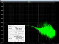
Finally the FFT of a 1kHz transient sim, which indicates a very low
distortion: the third harmonic is only 0.003% with 0.6Vp out - not
shappy.
Finally I have a confession to make. I have not build it - yet - as
I do not own an MC. Yet.
I've also designed a PSU to go with this, designed along the same
lines. Basically a shunt regulator, using a standard 12V AC wall wart.
I will probably present it in the Power Supplies forum soon
pls see attachment.
A lot has been added, relative to the simplified circuit. From left, I
have added 2 LTP in parrallel with the original, purely from noise
requirement. The reason for the BC639/BC640 is that a) it's readily
available and b) rumour has it, that they are merely BD139/140 in a
TO92 housing. In other words, medium power transistor, with a larger
chip compared to a normal small-signal one. I tried with 2sa1316 and
2sc3329 - they are specified as input transistors for MC amps, but
they sim worse - for what its worth - than BC639/BC640. The reason for
parelleling LTPs in stead of transistors is a practical on: it is much
easier to find 2 pairs than finding 4 transistors that match within,
say, 1mV from a batch of say 20 transistors.
MarsBravo: regarding R5/6 and R9/10, you are absolutely right. The
reason is that I some time ago bought 1000 pcs of 300 Ohms 1% for
next to nothing.
The next addition are Q7/8 (and Q15/16). Instead of a cascode, I
chose to use boot-strapping. There are two reasons for this.
Firstly, it is superior to the cascoding, as it maintains a constant
voltage over the boot-strapped transistor, Q6 an Q14. Secondly, the base
current flowing into Q7 cancels out the base current flowing out of
Q6, thereby improving the performance of the current mirror. R19 is
added to improve in this regard.
With a gain at LF/DC of 80dB, the output offset would be huge, even
with matched transistors. Even though I wanted to avoid using ICs,
I had to capitulate. I have not been able to come up with a simple
design for a servo. So hence the 2 OP-amps. The OP-amp here is LT1057,
but you could use OPA2134 or maybe even TL072. There is no reason to
use a very high spec (=expensive) OP-amp.
In stead of messing with the input transistors, I chose the approch
that you would find in OP-amps. Note the net labels BPA(Bias Positive A),
BPB(Bias Positive B), BNA (Bias Negative A), BNA (Bias Negative B),
which are also found in the current mirrors. Notice the output voltage
of the OP-amps: 2.2V and -2.2V respectively. In a real build, it might
be neccesary to reduce R30-R32.
Simulation results:
I've attached an AC plot of the RIAA accuracy : in short it's within
0.1dB from app 3Hz to 37kHz.
You'll also find a noise-plot which shows, that the primary noise
source is the MC-resistance (blue trace), #2 is the input-
transistors - there are 8, and I've only included one (red trace),
and #3 are the emitter resistors of the current mirrors (turquoise
trace), again only one is included. I'm afraid I'm not a noise master,
but it seems to me it could be worse. It may make sence to use
ZTX851/ZTX951 as Hans suggested.
Finally the FFT of a 1kHz transient sim, which indicates a very low
distortion: the third harmonic is only 0.003% with 0.6Vp out - not
shappy.
Finally I have a confession to make. I have not build it - yet - as
I do not own an MC. Yet.
I've also designed a PSU to go with this, designed along the same
lines. Basically a shunt regulator, using a standard 12V AC wall wart.
I will probably present it in the Power Supplies forum soon
Attachments
A few comments on your current latest circuit diagram:With a gain at LF/DC of 80dB, the output offset would be huge, even
with matched transistors. Even though I wanted to avoid using ICs,
I had to capitulate. I have not been able to come up with a simple
design for a servo. So hence the 2 OP-amps. The OP-amp here is LT1057,
but you could use OPA2134 or maybe even TL072. There is no reason to
use a very high spec (=expensive) OP-amp.
In stead of messing with the input transistors, I chose the approch
that you would find in OP-amps. Note the net labels BPA(Bias Positive A),
BPB(Bias Positive B), BNA (Bias Negative A), BNA (Bias Negative B),
which are also found in the current mirrors. Notice the output voltage
of the OP-amps: 2.2V and -2.2V respectively. In a real build, it might
be neccesary to reduce R30-R32.
Simulation results:
I've attached an AC plot of the RIAA accuracy : in short it's within
0.1dB from app 3Hz to 37kHz.
You'll also find a noise-plot which shows, that the primary noise
source is the MC-resistance (blue trace), #2 is the input-
transistors - there are 8, and I've only included one (red trace),
and #3 are the emitter resistors of the current mirrors (turquoise
trace), again only one is included. I'm afraid I'm not a noise master,
but it seems to me it could be worse. It may make sence to use
ZTX851/ZTX951 as Hans suggested.
Finally the FFT of a 1kHz transient sim, which indicates a very low
distortion: the third harmonic is only 0.003% with 0.6Vp out - not
shappy.
Finally I have a confession to make. I have not build it - yet - as
I do not own an MC. Yet.
Even if the BC139 is a BD139 etc, the spice model shows a Rb=0.5 Ohm.
No transistors have lower Rb's as the ZTX851/951 series with resp 1.2 and 1.5 Ohm, according to Horowitz & Hill, so be very sceptical with the outcome of your simulation.
Your input circuit looks very complex with that many transistors.
With the ZTX transistors and 7R Cart you wil have 0.5nV/rtHz RTI noise, that becomes 0.35nV/rtHz for a short circuited input.
More than adequate for 99% of the MC Carts.
My experience with the ZTX trannies is that they are all within 1mV Vbe.
You correctly named the extension with Q8, Q16 bootstrapping, this is of course also a version of cascoding.
You used a practical version keeping currents together.
The measured contribution of the current mirror emitter resistors seems a bit unlikely.
Counterintuitive, increasing their values will even result in a overall noise decrease of a few percent and vice versa.
And as a last comment, I find your servo overcomplicated. I didn't simulate it but it looks like a potentially unstable circuit, two servo's to solve one problem can fight each other.
Hans
A differential pair input stage automatically has 3dB more voltage noise than single-ended class A, since they are in series from a noise perspective.
The way the input transistors (ZTX851/ZTX951) are connected in this circuit (I forget the name of this configuration), reduces the voltage noise by 3dB as they are in parallel from a noise perspective which is much better for an MC amp: MC Phono Preamp
(note the configuration doesn't need feedback, that circuit happens to use it).
Last edited:
Hans, you are most likely correct with respect to the noise mechanics. As I said, I'm not a master in the noise department.
Regarding the servo: that is *not* two servos, only U1 acts as a servo, U2 is merely an inverter to give the right polarity for the bias. As it is a symmetrical amplifier without feedback, the servo must act on both the positive as well as the negative part.
Lars
Regarding the servo: that is *not* two servos, only U1 acts as a servo, U2 is merely an inverter to give the right polarity for the bias. As it is a symmetrical amplifier without feedback, the servo must act on both the positive as well as the negative part.
Lars
BTW this is a feedback amp anyway isn't it?, the RIAA network forms a current feedback path through the cartridge impedance.
Mark, you are absolutely correct. That is the price you have to pay, if you want to avoid large electrolytes in signal path.
My design is basically 4 Long tail pairs, 2 NPN- and 2 PNP-based in parallel. From a noise perspective it is equal to 2 parallel transistors in single ended configuration. So 4 times as many transistors in order to avoid the electrolytes.
Lars
My design is basically 4 Long tail pairs, 2 NPN- and 2 PNP-based in parallel. From a noise perspective it is equal to 2 parallel transistors in single ended configuration. So 4 times as many transistors in order to avoid the electrolytes.
Lars
BTW this is a feedback amp anyway isn't it?, the RIAA network forms a current feedback path through the cartridge impedance.
No it is not. Hence the elaborate servo.
I should have drawn it differently, what you see as a feedback, is in fact ground.
It is an transconductance amplifier driving the RIAA network. The only feedback is the servo to set the correct output voltage (=0V)
Lars
Last edited:
BTW this is a feedback amp anyway isn't it?, the RIAA network forms a current feedback path through the cartridge impedance.
Mark,
Where do you see a current feedback ?
I see no feedback at all, just a voltage to current converter, loaded with a Riaa network and followed by a buffer.
It has many of the ingredients of a CFA but it is not in this case.
Hans
That kind of IV converter is made by feedback. The input current to output voltage ratio is set by passives (the RIAA network, cartridge impedance, 300 ohm resistor etc), and the spare gain of the differential amp is turned into more linearity.
To convert current to voltage without feedback you need to pass the current through a resistive load and amplify the voltage difference across it. Then pass that signal through a passive RIAA network.
Creating any kind of virtual ground is a feedback trick.
To convert current to voltage without feedback you need to pass the current through a resistive load and amplify the voltage difference across it. Then pass that signal through a passive RIAA network.
Creating any kind of virtual ground is a feedback trick.
That kind of IV converter is made by feedback. The input current to output voltage ratio is set by passives (the RIAA network, cartridge impedance, 300 ohm resistor etc), and the spare gain of the differential amp is turned into more linearity.
To convert current to voltage without feedback you need to pass the current through a resistive load and amplify the voltage difference across it. Then pass that signal through a passive RIAA network.
It is *not* an IV converter, it is a VI converter . The input (i.e. the LTPs) converts the voltage from the cartridge to current witch in turn is mirrored and amplified as a current and send to the RIAA network, which convert it to a voltage .
Creating any kind of virtual ground is a feedback trick.[/QUOTE said:I'm afraid you have misunderstood the design. Pls go back to post #1 and reexamine the concept- and the simplified-schematics. There is no virtual ground and absolutely no feedback "trick". The only feedback is the servo to keep the DC on the output at 0, it has no bearing in the audio band.
Lars
Ah, poorly laid out schematic confused me - if one side of the diff amp is grounded but not obviously, why tie it to the RIAA network? You shouldn't have to chase down long nets looking for a single ground symbol somewhere along its length, ground symbol at every grounding point, unrelated circuit sections should have separate ground symbols.
Ah, poorly laid out schematic confused me - if one side of the diff amp is grounded but not obviously, why tie it to the RIAA network? You shouldn't have to chase down long nets looking for a single ground symbol somewhere along its length, ground symbol at every grounding point, unrelated circuit sections should have separate ground symbols.
Quite patronizing to tell others how to lay out their schematic as an attempt to mask your misjudgement.
Hans
Just reporting that it misled me. That's a statement of fact, followed by advice how to do better schematics (go check out Horowitz and Hill for where I learnt good practice here), so that others are less likely to be misled.
I admitted to a mistake, and analyzed why it happened, and offered ways to reduce the chances of such mistakes happening. That's trying to help people be less confused and less confusing.
If that makes you feel patronized I'm sorry, that wasn't my intention.
Analyzing mistakes helps prevent future mistakes.
... ... ... ... .... unrelated circuit sections should have separate ground symbols.
Agree.
Or rather: a manufacturer can draw it any way possible; many make no effort to make it easy for the service staff.
However a "teaching" diagram should be as clear as reasonably possible.
But if it isn't, I'll just move on un-taught. As I've done here.
- Home
- Source & Line
- Analogue Source
- MC 2 Line