syn08 said:
Ro=VA/Ic has nothing to do with degeneration. Its the basic bipolar transistor output impedance, a resistor connected between the collector and emitter.
Yes if to speak about the transistor itself, but an output resistance of the stage would be increased with degeneration that is a negative feedback by current. Also, the linearity will depend less on beta variations with currents and voltages, as the result.
Hi,
maybe I should not make any comment here as I have not read much of this, however the voltage gain is simply Rc/Re, (can`t be simpler).
maybe I should not make any comment here as I have not read much of this, however the voltage gain is simply Rc/Re, (can`t be simpler).
Lumba Ogir said:Hi,
maybe I should not make any comment here as I have not read much of this, however the voltage gain is simply Rc/Re, (can`t be simpler).
Sure, it is the close to this ratio the higher is Beta,.
Power gain with no degeneration is -Beta*Va/Vt
However, if to drive it by zero resistance voltage source, what are you amplifying then? Use a transformer. 😉
However, if to drive it by zero resistance voltage source, what are you amplifying then? Use a transformer. 😉
syn08 said:
Glen,
Ro=VA/Ic has nothing to do with degeneration. Its the basic bipolar transistor output impedance, a resistor connected between the collector and emitter.
I interpret your sudden silence on this matter to mean Oops! 😀
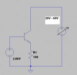
Attached is a less extreme example of a transistor biased at 20mA, with a 100 ohm emitter degeneration resistor. Lets suppose again that the transistors early voltage is 100V.
If the collector voltage source is varied from 20V to 40V, how much will the collector current vary?
Are you still going to maintain that the transistor looks like a 5k resistor, connected between the collector and emitter?
Attachments
G.Kleinschmidt said:
I interpret your sudden silence on this matter to mean Oops! 😀
Attached is a less extreme example of a transistor biased at 20mA, with a 100 ohm emitter degeneration resistor. Lets suppose again that the transistors early voltage is 100V.
If the collector voltage source is varied from 20V to 40V, how much will the collector current vary?
Are you still going to maintain that the transistor looks like a 5k resistor, connected between the collector and emitter?
Glen,
You need to get a better understanding of the differences between the large signal (including DC) models and the small signal (AC) models.
For DC and large signal, a valid model is e.g. Gummel Poon. For the small sinal (always linear) e.g. the Giacoletto hybrid PI model, or quadripole hij etc... model applies.
There is little to none connection between these two models, except the fact that the small signal parameters are depending on the bias point as well. E.g. the impedance between the emitter and the base is Beta/Gm, Gm=Ic/Vt, the impedance between the collector and the emitter is Ro=VA/Ic.
From this perspective, for small AC signals, there is a 5k resistor between the collector and the emitter and everything I said holds. Spice uses a hybrid PI model for the AC analysis and the Gummel Poon model for the DC and transient analysis (both non linear, large signal analysis). When you are determining the ULG, etc... you are in fact using the small signal, linearized, BJT model.
For further details about the large and small signal models here's a good starting point:
http://ecee.colorado.edu/~bart/book/book/chapter5/ch5_6.htm
Ooops, sorry, I just lectured you... 🙂

syn08 said:From this perspective, for small AC signals, there is a 5k resistor between the collector and the emitter and everything I said holds.
Well I maintain that everything you said certainly does not hold and you are avoiding my rather simple question.
For ac signals the collector impedance is a great deal larger than 5k.
You were wrong in another thread when you told Waveborn that the collector (output) impedance of his current mirror was simply equal to VA/Ie, and, as far as I can see, you have made the same mistake here.
And your calculation above that determines that the “LF gain” of the Otala VAS “is about 670 or 56dB” with the two 2.2k load resistors (which is, in reality, a little over 20, or ~26dB) simply makes no sense whatsoever.
Now lets get back to my example. I've got a 1kHz sinusoidal voltage on the collector with a DC offset (varying from 20V peak to 40V peak). There's an AC component there to make you happy.
Please tell me how much the collector current varies.
My rule of thumb is the real part of the output impedance varies from Va/Ic to Beta*Va/Ic depending on how many Vt's of degeneration you have in the emitter. YMMV.
This bit us on an very old current mode in-amp where the process fundamental (Beta,Va product) moved 2X causing 100% failure to the non-linearity spec.
This bit us on an very old current mode in-amp where the process fundamental (Beta,Va product) moved 2X causing 100% failure to the non-linearity spec.
scott wurcer said:My rule of thumb is the real part of the output impedance varies from Va/Ic to Beta*Va/Ic depending on how many Vt's of degeneration you have in the emitter. YMMV.
Thankyou Scott. That is indeed quite some range. But what is a "t"?
G.Kleinschmidt said:
Thankyou Scott. That is indeed quite some range. But what is a "t"?
It is a letter in Vt that means Thermal Voltage, that is K*T/q where K = Bolzman's constant, T is an absolute temperature, q is an electron's charge.
Reminds me, "Do you know why train's wheels knock? Because they are round. Their area is pi*r^2, i.e. proportional to squared root. That squares knock"
Yes VT is the thermal voltage .0259V or so at 300K. The point is a cascoded current source still loses current via the base current (beta modulation) even though there are effectively "infinite" VT's of degeneration.
scott wurcer said:Yes VT is the thermal voltage .0259V or so at 300K. The point is a cascoded current source still loses current via the base current (beta modulation) even though there are effectively "infinite" VT's of degeneration.
OK, 😎 That makes perfect sense.
G.Kleinschmidt said:
For ac signals the collector impedance is a great deal larger than 5k.
Glen,
If by "collector impedance" you mean the "small signal output impedance" then you are correct. It would certainly help if you would brush a little your listening/careful reading skills; First, Ro IS NOT the output impedance. Ro is the impedance between the collector and the emitter that models the Early effect.
You changed "a little" the problem, now you are asking for the OUTPUT IMPEDANCE of a degenerated common emitter circuit. The answer is (with a small approximation):
(1) Zo=Ro*(1+Gm*(Rb'e||Re))
Before plugging in some numbers, please note that the effective degeneration is NOT Re alone, it is Re||Rb'e. And now, some numbers:
Ic=20mA
VA=100V
Beta=100
Re=100ohm
Then:
Gm=Ic/Vt=20mA/0.026V~800mA/V
Rb'e=Beta/Gm=100/800mA/V=125ohm
Ro=100V/20mA=5kohm
Rb'e||Re~56ohm
Note that the effective degeneration is about half the 100 ohm resistor, and that's simply because of the low Beta and high collector current.
Therefore:
Zo=5kohm*(1+800mA/V*0.056kohm)=5kohm*46.8 that is about 240kohm.
This lies between what Scott mentioned as a rule of thumb.
Now, back to Wavebourn's high current mirror, you would of course note that, in terms of the small signal output impedance, the degeneration is less effective when the collector current rises. Assuming a 200mA current mirror, and using the same numbers as above, the effective degeneration resistor would be only 10ohm! And you can increase the emitter resistor Re until the cows come home, this won't help a iota. Combine this fact with a low Ro (because of the high collector current) and assuming the same numbers as above, the output impedance will be no larger than 50kohm. To me this is crap, but YMMV. Of course, the solution is to use high Beta devices and also high Early voltage devices. Now, for a low current current mirror, the degeneration is controlled by Re and changing Re may significantly change the output impedance. Of course, the higher Re the higher the output impedance.
What I was talking re: gain was always referred as "intrinsic gain", not the gain of the entire stage. But that's already a different story, it's 4AM in the morning here, I need to get some sleep 🙂 A final note: you can re-arrange (1) above and put it in the Y=Yo*A/(1+F*A) where Y stands to the output conductance and identify F; this would be the feedback view of a degenerated common emitter circuit. You could then identify when, from a feedback perspective, is the local feedback loop gain large enough to consider Y=Yo/F a valid approximation (as a function of the device bias and intrinsic parameters). Very interesting exercise!
scott wurcer said:Yes VT is the thermal voltage .0259V or so at 300K. The point is a cascoded current source still loses current via the base current (beta modulation) even though there are effectively "infinite" VT's of degeneration.
OK, Vt should have been obvious. My text books and school texts have been doing me a disservice here as they just call Vt "25mV" 😀
But back to beta limiting the output impedance with infinite Vt degeneration. Wouldn't it be more acurate to say that it is the beta non-linearity that is the limiting factor?
Correct me if I'm wrong, but if beta was perfectly constant with Ic, I can't see how it could limit the output impedance.
Attachments

syn08 said:
If by "collector impedance" you mean the "small signal output impedance" then you are correct. It would certainly help if you would brush a little your listening/careful reading skills; First, Ro IS NOT the output impedance. Ro is the impedance between the collector and the emitter that models the Early effect.
You changed "a little" the problem, now you are asking for the OUTPUT IMPEDANCE of a degenerated common emitter circuit. The answer is (with a small approximation):
Well what else are we talking about, besides the "small signal output impedance"?
And how did I change the problem? The Otala VAS IS AN EMITTER DEGENERATED COMMON EMITTER CIRCUIT!
And you defined the output impedance of the Otala VAS as being equal to Ro (VA/Ic) - 5k per side and 2.5k for the push-pull (Va=100V, Ic=20mA) Remember????
For basic analysis I even specifically gave you a common emitter circuit equal to one half of the Otala VAS, with its 100 ohm emitter degeneration resistor and 20mA bias current (which is degenerated to approximately 77 Vt's, BTW)!
Your "intrinsic gain" calculations of the Otala VAS are still wrong and pointless to me.
The LF voltage gain of the Otala VAS is simply equal to
2 * (1.1k / (100R+Remitter))
Where 1.1k is the two parallel 2k2 VAS load resistors (R26 and R27)
100R is the emitter degeneration (R18 and R19)
And Remitter is the internal emitter resistance of the transistors.
This is multiplied by 2 because there are two such common emitter stages with the degeneration+emitter resistances effectively operating in parallel.
The answer is a little under 22Av, or ~27dB. This is pretty basic stuff.
I honestly believe your are a bit too wrapped up in your algebra to see the forrest for the trees.
Now I have other things to do as well, namely cooking and eating dinner.
- Home
- Amplifiers
- Solid State
- Matti Otala - An Amplifier Milestone. Dead or Alive