I can test with TC-1 but i don't have spare though i can make a swap of Q6025 L-CH and Q6026 R-CH
to confirm if high DC problem move with Q6025 to Right chanel 😊
desoldering time
should i replace 43K resistor with wanted 47K one ?
thanks
to confirm if high DC problem move with Q6025 to Right chanel 😊
desoldering time
should i replace 43K resistor with wanted 47K one ?
thanks
Your call on both. However, I would not mess with the 43k until the amp is otherwise working--- we don't need to introduce any additional uncertainties.
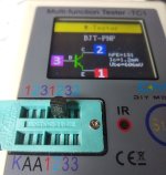
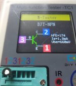
tests Q6025 and Q6026 seems twins ok to me
131 to 135 HFE
1,2 to 1,3ma
604 to 606 Ube
and to confirm after swap no change
still High DC -2.6V on Left Chanel
and litlle DC 0,1V on Right Chanel
this is making me
i'm making mv mesurements on Right chanel to compare...
thanks for your help
131 to 135 HFE
1,2 to 1,3ma
604 to 606 Ube
and to confirm after swap no change
still High DC -2.6V on Left Chanel
and litlle DC 0,1V on Right Chanel
this is making me
i'm making mv mesurements on Right chanel to compare...
thanks for your help
Attachments

Last edited:
Very worthwhile experiment! You have good instincts. I imagine the behavior at the collectors is still about the same.
To my eyes, the Q6023, 25, 27, 29 transistors implement relatively straightforward adjustable current sources, yet they don't seem to behave. Would you examine the wiper voltage at V6003? It should range about +/- 1.8V.
I'm contemplating another, bolder experiment.
To my eyes, the Q6023, 25, 27, 29 transistors implement relatively straightforward adjustable current sources, yet they don't seem to behave. Would you examine the wiper voltage at V6003? It should range about +/- 1.8V.
I'm contemplating another, bolder experiment.
Thanks.
So please explore how the the emitter voltages at the above transistors change as you adjust VR6003. Q6027 base-emitter junction should largely cancel the base-emitter junction of Q6023; if you measure voltage between emitter of Q6023 and the pot wiper, I believe it will be a few tens of mV at most and vary smoothly with wiper position. Very smiliar behavior should appear at emitter of Q6025. Compare with the other channel if any suspicion. Maybe a defect will be revealed.
The bolder experiment is to lift the end of R6043 that is tied to D6005 and instead connect R6043 to the positive rail. Perform the same operation on R6045 to connect it to the negative rail. Now we can investigate the offset bias independently of the front end. I think the problem lies in one of these two areas.
Hello,
thanks !
here is all voltage measurement from transistor emitter to wiper
Left chanel (out of pot range -2,6V High DC presence):
Q6023 ....... V6003(dc offset adjust)........ V6001 (bias adjust)
CW ...... 1,340v ..................... 4,752v
CCW...... -1,696v .................... 4,160v
Q6025
CW...... 1,421v ....................... 4,647
CCW...... -1,635v .......................... 4,092
Right Chanel (bias pot manageable 0,1V DC presence):
Q6026 V6004(dc offset adjust)..... V6002 (bias adjust)
CW..... 1,496v ........................... 2,100v
CCW....... -1,494v ........................... 1,504v
Q6024
CW...... 1,472v ............................ 2,116
CCW...... -1,526v ............................ 1,532
Bias pot wiper to emitter show near double voltage on left compared to right side ... does this help to locate culprite zone or compoents ?
For the bolder experiment can you please confirm i understood ok?
here is after R6043 wiring correction (same to do on negative rail with R6045)
Last edited:

Hi Phil,
Sorry for delay in responding.
Well I made two serious errors in my previous request for data. I was intending to ask for tracking of emitter voltages with respect to base voltage of Q6027, but that's not what I wrote. 😕 Second error was misreading schematic and not recognizing that R6061 is connected to amp output, which raises feedback complexity. 😕
So I've created a table below to attempt better organizing the data and have entered some data taken from earlier posts. Would confirm my entries, especially that I have rotation of the pot correct? Once table is correct, would you fill the missing dats entries?
Sorry for leading you to the wrong measurement points. Please defer the "bold experiment" until it becomes more appropriate.
Thanks,
Steve
From post 9:
V6003 Left-CH gives -2.65V initial, adjustement range from -2.82V to -2.10V so impossible to go down more than -2.1V full anticlockwise,
From post 18:
mesurement requested
with V6003 full Clock Wise vs anti-CW
Q6023 collector Voltage 11,867 to 16,133v
Q6025 collector Voltage -36,701 to -35,961v
| VR6003 wiper | Q6029 base | Q6023 emitter | Q6023 collector | Q6025 emitter | Q6025 collector | L_CH (output) |
| +1.524(cw ?) | 11.867 (cw) | -36.701 (cw) | -2.82 (cw) | |||
| -1.523 (acw ?) | 16.113 (acw) | -35.961 (acw) | -2.10 (acw) |
no problem Steve 👍
thanks a lot for your precious help and please don't apologise, there is no need to as no delay to respect here for me.
i'm screwed since few weeks being deseperate to fail with this repair, so i'm very glad and appreciate your kind help and all i learn
thanks for such smart idea, i will make measurements and complete your useful table !
sorry for silly question the other test point must be ground right ?
Here it is completed, thanks
| VR6003 wiper | Q6029 base | Q6023 emitter | Q6023 collector | Q6025 emitter | Q6025 collector | L_CH (output) |
| +1.539 CW | 0,216 steady | 0,206 steady | 12,240 to 12,362 | 0,123 steady | -36,406 to -36,673 | -2,725 |
| -1.525 ACW | 0,162 steady | 0,162 steady | 17,260 to 17,353 | 0,097 steady | -35.887 to -36,063 | -2.129 |
From the data, I would have said Q6025 had failed, but you tested the transistor and swapped channels, so that seems unlikely.
You could perform the same table experiment on the other channel for comparison, but the picture will be be distorted because the right channel output responds to the adjustment pot, but L_CH seems stuck in ~ +2V territory. So your call re doing that exercise.
So it may be time for the bold experiment. The amp output is likely to shift when this experiment is tried, so that will further change the feedback presented to R6061. Consequently, you may need to lift one end of R6061; the offset pot should still be sufficient to manipulate the current sources to both polarities, the objective being to exercise the collector voltages as a test of the current sources. The front end should still respond to input signals if it's not broken (albeit with unknown offset) and should be easier to diagnose without the uncertainties of the offset network.
The right channel data looks much better, doesn't it?
Note that the right channel has an adjustment range of 0.598V, and the left channel has 0.556V, nearly as large, but not centered near enough to 0V to allow nulling. The right channel shows 27mV variation at Q6030 base; the left channel shows 54mV variation at Q6029 base.
I think this data supports the bold experiment, and disabling the R6061 path will probably also be necessary. I anticipate that exercising the pot will demonstrate ample control range on both Q6024 and Q6026 collectors. I believe the underlying problem is in the input stages and we'll tackle that when operation of the current sources is absolved of fault.
thanks for your expertise
i see similarities at 0V base and emitters, lower voltage supply rails though more twined than on disparate L-CH so if it's ok for you it's ok for me 😊
i'm pulverising some electronic contacts de-oxydant on potentiometers, will do no harm...
Ready to go for bold experiment + R6061 path disabling, do i have to do same on right chanel ?
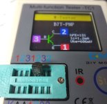
before bolder experiment i decided testing (only HFE is not matching well) and swapping Q6023 and Q6024 > no change high DC is always on Left,
will do the same with Q6027 and Q6028 and if no change will go to your advise 😉
A question please
if there is one what's the différence between 2SA1266 Y and no Y transistor ?
will do the same with Q6027 and Q6028 and if no change will go to your advise 😉
A question please
if there is one what's the différence between 2SA1266 Y and no Y transistor ?
Attachments
Last edited:
- Home
- Amplifiers
- Solid State
- Marantz PM5000 DC offset voltage > protect mode