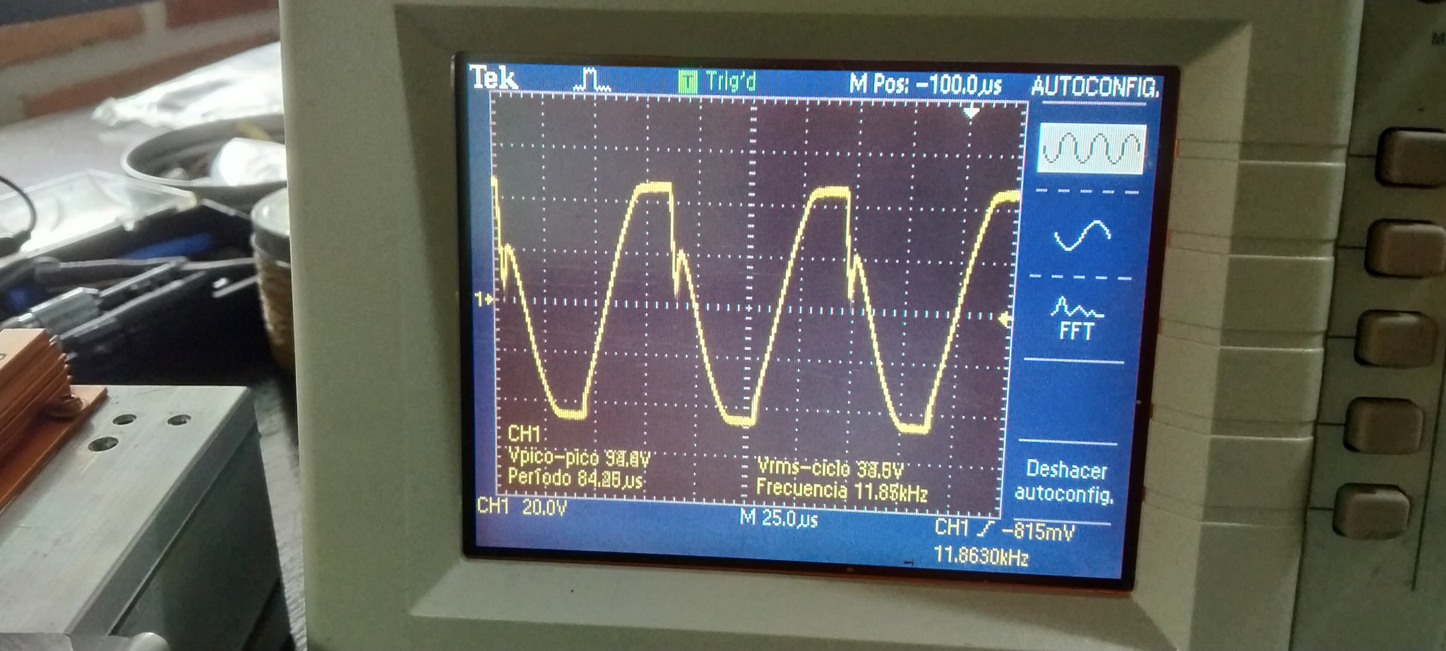
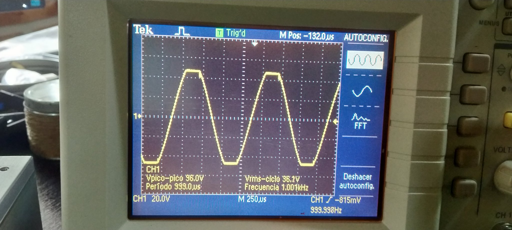
Just finished rebuilding it. One board was burnt. After rebuilding both boards, I'm testing it and it works fine, except when clipping, as can be seen in the pictures. At low frequencies seems to clip clean or I cant see it, but on higher frequencies does this(8ohm load):


I have replaced almost every transistor in both boards, because the blown board had most of them bad. Both boards behave the same. And important to mention, they were modified like the ones on this thread:
https://audiokarma.org/forums/index.php?threads/some-info-on-my-250m-please.744954/
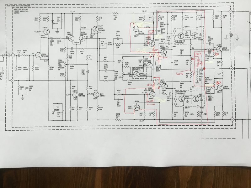
As it seems that modification appears to be factory made, because looks exactly made as the ones on the thread, I didn't undo it. Apparently, it replaces the current limiting adjustment pots, someone draw the mod, but I think it is not totally correct, there are at least two diodes that doesn't appear:

As said, if you don't drive it to clipping, everything seems ok, but I don't like that waveform at clipping, and don't know if it is a recovery problem, or it is caused by the modification to the current limiting circuit, and what can I do to eliminate it.
I have replaced almost every transistor in both boards, because the blown board had most of them bad. Both boards behave the same. And important to mention, they were modified like the ones on this thread:
https://audiokarma.org/forums/index.php?threads/some-info-on-my-250m-please.744954/
As it seems that modification appears to be factory made, because looks exactly made as the ones on the thread, I didn't undo it. Apparently, it replaces the current limiting adjustment pots, someone draw the mod, but I think it is not totally correct, there are at least two diodes that doesn't appear:
As said, if you don't drive it to clipping, everything seems ok, but I don't like that waveform at clipping, and don't know if it is a recovery problem, or it is caused by the modification to the current limiting circuit, and what can I do to eliminate it.
No intention to contradict Bonsai, but I can confirm that the clipping signal in post 1
is as expected and checked it today on my workbench with model 250M no. 3023.
The picture shows a high frequency of 12 kHz and you probably remember to see
similar behaviour with op amps of the same era. You can not expect hf brilliance
from transistors manufactured 50 years ago.
is as expected and checked it today on my workbench with model 250M no. 3023.
The picture shows a high frequency of 12 kHz and you probably remember to see
similar behaviour with op amps of the same era. You can not expect hf brilliance
from transistors manufactured 50 years ago.
Better schematic here : https://www.diyaudio.com/community/threads/marantz-250m-bias-throws-dc-offset-off.347032/
This is a "complementary darlington", also called "compound pair" emitter follower at the input.
They must have considered it useful for connection to a tube preamp of the time.
I fail to see 1k resistors at the output device collectors.
This is a "complementary darlington", also called "compound pair" emitter follower at the input.
They must have considered it useful for connection to a tube preamp of the time.
I fail to see 1k resistors at the output device collectors.
At low frequencies seems to clip clean or I cant see it
latch-up is there, but your course display is helping to hide it, zoom in
Output stage is common collector. It’s a variation of CFP with gain. They are KNOWN to be problematic. Oscillation, latch up, reverse breakdown of emitter-base. You name it, it happens, unless pains are taken in the design to prevent it all.This schematic makes my brain hurt. What an unusual design.
For instance that weird 2-transistor 'input stage' before the actual input stage.
And the output stage just can't be drawn right. 1K Ohm resistors at the collectors of a power amp?
Those transustirs with the 1k’s in the collector are the over current protect.
Looking @ the scope pictures, they show some hangup both pos & neg @ 1k. The 12k is way more hangup. I would remove the load and see if the clipping is good. If good, add the load back on and I would try to adjust the over current adjustments (250m schematic).
I would also do a frequency & phase plots with load & no load for more details of real performance.
Duke
I would also do a frequency & phase plots with load & no load for more details of real performance.
Duke
This Marantz circuit is very prone to common mode conduction and that is what you are seeing on your scope. I have repaired too many of these amplifiers and the cure is simple.
To illustrate how crude the design is, just look at how much compensation there is around the output stage AND it is not symmetrical.
The VAS stage Q507, Q508 use reasonable fast devices and they need Miller compensation. They carry 12.7mA at idle and this changes as the power supply droops (Another dumb design)
100pF collector-base of each device will cure some of the issues.
Marantz tried to use a 1000pF shunt capacitor C512 from the VAS to ground. Reduce this to 220pF.
The VAS drives Q510 and Q511. Insert base stoppers into these transistors of about 47R-68R and this really helps. Again these TO66 devices are quite fast. I normally replace them with MJE15030/MJE15031 if blown.
Each output device should also have base stoppers of between 2R7 to 5R6 1watt.
Nigel Wright wrote :
If it only does it when clipping then I wouldn't worry about it.
Other than that check VAS capacitor and maybe increase a little.
Nigel there are NO VAS Miller capacitors!!!!!!!!!!!!!!!
AS Audio wrote:
You can not expect hf brilliance
from transistors manufactured 50 years ago.
Really where did you pull this from?
Cvanc wrote:
This schematic makes my brain hurt. What an unusual design.
For instance that weird 2-transistor 'input stage' before the actual input stage. Not weird they wanted to add circuitry to look clever
And the output stage just can't be drawn right. 1K Ohm resistors at the collectors of a power amp? mmmm schematic reading!!!
Most of our clients who bring these 250s to us for restoration we always remove the drive boards and replace them with my full complementary design with "normal" emitter follower triple output stage so we do not have to deal with the issue which we see others do.
Throw out the 20,000mfd 60v caps and replace with 47,000mfd and add in surge circuit on the mains to ensure low turn on current.
Steve
Zed Audio Corp.
The input stage is a high impedance buffer (emitter-follower + CCS), the transistors on the right aren't the power transistors, they are probably current limiters to protect the output devices which are parallel pairs marked as off-board (ie on the heatsink).This schematic makes my brain hurt. What an unusual design.
For instance that weird 2-transistor 'input stage' before the actual input stage.
And the output stage just can't be drawn right. 1K Ohm resistors at the collectors of a power amp?
No, this is not a current source, see post 7.The input stage is a high impedance buffer (emitter-follower + CCS), the transistors on the right aren't the power transistors, they are probably current limiters to protect the output devices which are parallel pairs marked as off-board (ie on the heatsink).
Q516, Q517 limit drive current.
- Home
- Amplifiers
- Solid State
- Marantz 250M clipping artifacts