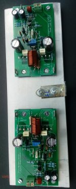
I designed the PCB for Maplin Mosfet amp which is in fact modified Hitachi app note circuit. I tested it with 30V supply because it's the limit of my lab PSU. The square, sine and triangle were perfect on the scope but DC offset is -106mV on both channels. I am perplexed because I matched the input transisitors to have low offset. What could be the problem? The amp is designed for 50V supply.
-106mv isn't that bad when you consider the era this amp is from and the fact we attached less importance to such things.
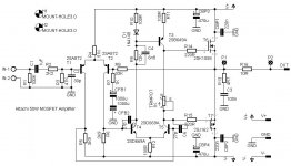
The most obvious cause of offset in this amp is the unbalanced feedback resistor vs input resistor which is R2 and R7. The input resistor should equal the feedback value (33k). If that and the input transistors are matched then the offset should be pretty low.
The most obvious cause of offset in this amp is the unbalanced feedback resistor vs input resistor which is R2 and R7. The input resistor should equal the feedback value (33k). If that and the input transistors are matched then the offset should be pretty low.
Feedback resistor and input resistor are equal, 47k. Even gain setting resistor and series input resistors are equal, 1k. Input transistors are matched. This was the first power amp PCB I designed few months ago when I learned to use EAGLE PCB software. I know that even -106mV is tolerable but with all the measures I applied I was surprised to see the level of DC offset.
Attachments
All you can do in this case is try different transistors in the front end and not match them so closely. You can also try altering the input resistor a little. I think increasing it will pull the offset more positive.
Maybe go back to the 33k feedback value (that is what my Maplin circuit shows) and increase R2. Perhaps the imbalance was deliberate to overcome a known design limitation. Slightly mismatched transistors should make a massive difference though.
Maybe go back to the 33k feedback value (that is what my Maplin circuit shows) and increase R2. Perhaps the imbalance was deliberate to overcome a known design limitation. Slightly mismatched transistors should make a massive difference though.
I built a number of these 100W Maplin amplifiers, back in the old days and overcame this issue by selecting matched PNP transistors for TR1 and TR2.
I built a number of these 100W Maplin amplifiers, back in the old days and overcame this issue by selecting matched PNP transistors for TR1 and TR2.
yep ... exactly what I do
Mine are below 20mv
Is it 30V total from V+ to V- or you used + and - 30V rails?
30V total could be to low and cause the excessive DC offset. What is the voltage difference between bases of the transistors consisting the first and the second diff pair?
30V total could be to low and cause the excessive DC offset. What is the voltage difference between bases of the transistors consisting the first and the second diff pair?
Last edited:
chip_mk,
Lab PSU I used was at +/-30V (60Vp/p), the uper limit of my lab PSU. Since the circuit was originally designed for +/-50V, my first impression was that low supply voltage could be the culprit for high DC offset. When I test the amp with proper supply voltage I shall report if that was indeed the culprit.
Lab PSU I used was at +/-30V (60Vp/p), the uper limit of my lab PSU. Since the circuit was originally designed for +/-50V, my first impression was that low supply voltage could be the culprit for high DC offset. When I test the amp with proper supply voltage I shall report if that was indeed the culprit.
Just to mention, my first Hitatchi clone of that basic topology was the "Winton" amp, a project published in "Galaksija" magazine in January 1981.
After so many years I return to it in my latest HPA project presented here CPLHF output stage
After so many years I return to it in my latest HPA project presented here CPLHF output stage
Voltages at the bases of transisitors:
First pair KSA992
T1 2,1mV
T2 -65mV
Second pair 2SD667A
T4 -28,67V
T5 -28,72V
In the original Hitachi circuit input resistor was 47k and feedback resistor was 22k.
First pair KSA992
T1 2,1mV
T2 -65mV
Second pair 2SD667A
T4 -28,67V
T5 -28,72V
In the original Hitachi circuit input resistor was 47k and feedback resistor was 22k.
Last edited:
With this base voltage T1 should be completely turned off. And yet, both collector resistors receive similar current. Hmm...
Both DC offset and voltages at the bases of first and second pair are the same for both left and right channel pcb.
What about voltages across R10 and R11? They should be close in value. And what is the value of quiescent current?
Is it 30V total from V+ to V- or you used + and - 30V rails?
30V total could be to low and cause the excessive DC offset. What is the voltage difference between bases of the transistors consisting the first and the second diff pair?
I use the +50 - 50 voltage rails ... then I used the JLH regulated power supply module
regulated +/- 50 V rails and regulated +/- 55v rails for the power mosfets even better in my opinion
regards
And I have to add, DC offset is in some cases caused by oscilation. So this is also worth checking. Use auto function on the scope to try to catch something.
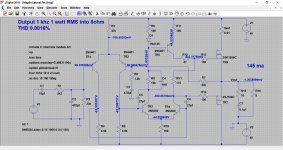
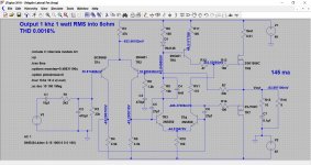
Quiescent current is 30mA. Please check my schematic for R10 and R11. My markings are different from markings on Maplin/Hitachi schematic. I did not notice any excessive heat on the components so I guess that amp is stable. My scope is only 20MHz so it is impossible to see some very high frequency oscillation.
Attachments
Last edited:
With this base voltage T1 should be completely turned off. And yet, both collector resistors receive similar current. Hmm...
It is the base to emitter differential that determines whether it is on or not. The base of TR1 can be grounded if desired, the DC conditions will remain correct as the emitters of the pair will be around 650 mv positive with respect to the base(s).
I remember the Winton amp. It appeared in Practical Wireless around 1980 I think at the time I was still at college and a friend built it. It was pretty good as I recall.
I wouldn't worry to much over the offset tbh, just pick a couple of transistors that get it nearer the mark... or leave it be 🙂

If all parts are OK and properly connected and the PCB is correctly routed then I tend to suspect a mismatch in the current mirror consisted of D1 and T3. I would try to replace D1 with another 2SB649A with shorted collector and base (transistor turned to diode).
- Status
- Not open for further replies.
- Home
- Amplifiers
- Solid State
- Maplin MOSFET amp DC offset problem