Hey folks, newcomer here after being a reader for a few years 👋
I’m working on small DIY DAP (imagine if iPod Shuffle and Shanling M0 had a baby) and after 1st prototype I’m trying to squeeze the best possible performance from the limited PCB space / orientation and will appreciate your help
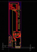
I did split design into multiple PCBs and arranged them into C-shape - you could see high freq. and audio parts + dimensions marked on the images attached:


I don’t have any experience designing top-notch audio PCBs (or low noise analog in general), so all extra opinions/thoughts are very welcome, but my main questions are:

In overall I want to create end game portable DAP with buttons 😄 So any drops of wisdom from you folks will really help to make it happen! 🙌
I’m working on small DIY DAP (imagine if iPod Shuffle and Shanling M0 had a baby) and after 1st prototype I’m trying to squeeze the best possible performance from the limited PCB space / orientation and will appreciate your help
I did split design into multiple PCBs and arranged them into C-shape - you could see high freq. and audio parts + dimensions marked on the images attached:
I don’t have any experience designing top-notch audio PCBs (or low noise analog in general), so all extra opinions/thoughts are very welcome, but my main questions are:
- I’ve used PCM5102A to just have I2S sound output - but does it make sense to use smth better? I’ve heard that biggest contributor to noise will be the rest of the design and getting better DAC with lower noise floor is not really worth it since the rest of the design won’t be able to go that low.
- What is the best amplification option to squeeze in here considering it will be for headphones only? I don’t drive anything demanding, but having some margin for the future will be useful.
- Any recommendation on analog parts (i.e. using smth else than mlcc caps, any specific manufacturer e.t.c.)? Any examples of best in class PCBs of similar size to learn from?
- If I will route audio signal from amp to jack on another PCB via headers - could that introduce significant extra noise?
- Is common PCB stackup S-G-G-S is okay or I could get extra shielding by using G-S-S-G? Considering that on DAC PCB below analog signal it will be mostly G-G-S-G since I doubt I would need 2 layers for analog part and will just pour 2nd signal as well.
- Will making PCB 0.8mm introduce some extra coupling that will be critical compared to 1.2mm stackup?
- Should I put some shielding on PCB with MCU? Like the ones that could be usually seen on ESP32 modules or on XIAO boards - thin metal enclosure wrapping top layer components to limit noise coupling to DAC PCB. Or it’s just way too far to influence another PCB?
- I plan to use connected ground planes - i.e. no separation between analog and digital. Or it’s a good idea to split them and then connect using ferrite beads and other voodoo magic?
- LDOs are the best choice for portable analog power source, right? Since buck & switching will introduce more noise.
- Using same LDO for DAC and MCU DVDD is okay, right? Only AVDD should have separate LDO to decouple from digital noise.
- Should I do vias stitching if I don't have any wireless onboard? Could that help shield any external noise or it's not an issue unless I add bluetooth.
- I have another option of stackup where PCBs will be on top of each other (”Parallel Stackup” image) - will that couple way too much noise from digital PCB?
In overall I want to create end game portable DAP with buttons 😄 So any drops of wisdom from you folks will really help to make it happen! 🙌
Last edited:
Looks like you are going about this is maybe not such a good way. Seems like there are a lot of assumptions baked into the questions you are asking, but the questions you aren't asking are perhaps the more telling.
How about this instead, show us the just the dac board schematic, and the rough proposed layout of devices that will go on the dac board including the location where power comes in to the board? How would you propose to connect the dac board ground plane to the ground planes of the other boards? Why or why not use any power planes?
Then consider in more general terms how you will isolate the dac both electrically and mechanically from the MCU. How will you manage both radiated and conducted EMI/RFI coupling from the MCU/display/digital storage, etc., to the sensitive analog dac circuitry (also considering that in dacs, clocks are included as sensitive analog circuitry).
Also, please describe your plans for how this will be powered, batteries recharged how and how often (with a wall wart?), data transferred to/from a PC or any other external devices. That's just in case any external connections could introduce noise/interference into the sensitive dac circuitry.
Then once some of the more sensitive circuitry has been thought through sufficiently, the start working from the dac board needs towards more detailed planning of coupling/interaction with the digital circuitry.
Just some thoughts for your consideration, is all.
Last edited:

Thanks for the reply Mark! I indeed likely have a lot of wrong assumptions about analog electronics since I coming from the low freq. digital world.
Here is the schematic, but as I did mention it's just a placeholder I've created to finalize software part for the mainboard and to see how it would feel to use in real life - so it's pretty basic and does not even have it's own LDO or any kind of amplification and just drives headphones directly from PCM5102.

I do plan to potentially move connector closer to the digital part and LDOs will be put close to DAC IC as well.
Grounds between PCBs connected via headers that connect boards together.
I didn't think any power planes were necessary - whole device will draw max 1 amp in total so I just routed power using thick enough traces on signal plane.
Power-wise it will be mainly from 14500/10440 battery and won't be used during charging so extra noise during charging is not an issue.
There is no display, so the only high freq part besides MCU is SD card and they are both about 10mm away from DAC PCB, but I'm not sure if that's far enough so no significant coupling will happen? But I'm not sure if that will have a major effect if I will stack PCBs on top of each other instead.
On data transfer - well, I'm thinking about adding a possibility to use it as USB DAC, in that case connection will be made via mainboard that has USB connector, but I'm not really sure if that's the feature I would add since my main usecase is listening on the go.
Does that make sense? If I'm missing smth or things are still not clear - please let me know 🙏
Here is the schematic, but as I did mention it's just a placeholder I've created to finalize software part for the mainboard and to see how it would feel to use in real life - so it's pretty basic and does not even have it's own LDO or any kind of amplification and just drives headphones directly from PCM5102.
I do plan to potentially move connector closer to the digital part and LDOs will be put close to DAC IC as well.
Grounds between PCBs connected via headers that connect boards together.
I didn't think any power planes were necessary - whole device will draw max 1 amp in total so I just routed power using thick enough traces on signal plane.
Power-wise it will be mainly from 14500/10440 battery and won't be used during charging so extra noise during charging is not an issue.
There is no display, so the only high freq part besides MCU is SD card and they are both about 10mm away from DAC PCB, but I'm not sure if that's far enough so no significant coupling will happen? But I'm not sure if that will have a major effect if I will stack PCBs on top of each other instead.
On data transfer - well, I'm thinking about adding a possibility to use it as USB DAC, in that case connection will be made via mainboard that has USB connector, but I'm not really sure if that's the feature I would add since my main usecase is listening on the go.
Does that make sense? If I'm missing smth or things are still not clear - please let me know 🙏
Attachments
Power (and ground) planes are mainly for low noise and low inductance.
https://www.amazon.com/High-Speed-Digital-Design-Handbook/dp/0133957241
https://www.amazon.com/High-Speed-Digital-Design-Handbook/dp/0133957241
A few words about dacs, if I may.
Master clocks should be located pretty much next to the dac chip, even if the particular dac chip doesn't use the MCLK signal. At least you can de-jitter the I2S signals that drive the dac using a reclocking technique. Jitter is a type of analog noise that can cause noise and distortion effects if not reasonably minimized; it is one of the two critical reference signals needed by any DAC or ADC. Same thing for Vref (aka AVCC, or whatever its called in a particular dac), which is the other critical reference signal needed by a dac. In addition, no part of the dac should be on the same voltage regulator as the MCU. Dac voltage regulators should be on the same board and ground plane as the dac chip.
The MCU should be behind isolator chips so that it can send isolated I2S to the dac (and isolated I2C, if needed). Also, isolated MCLK signals can be sent from the dac board to the MCU to act as a reference for the MCU.
Ground planes are necessary for controlled impedance transmission lines of RF signals. Power planes are useful for keeping power rails low impedance and with low voltage noise. Current flows in ground planes are something that should be considered since most unwanted stray coupling when using ground and power planes is magnetic, not electrostatic.
Also, output stages should be located on the same ground plane and same PCB as the dac chip. There should be a clear uninterrupted ground plane path between any I/V opamps (if used) and the dac chip.
There is more about clock switching, powering, bypassing, buffering, etc., but at least the above is maybe some stuff to start thinking about. Also, there is some explanation of a pretty well working clocking scheme shown at: https://www.diyaudio.com/community/threads/general-purpose-dac-clock-board.413001/post-7975729
Last edited:
Now I will add one more little thought: High speed digital design and dac design are not exactly the same thing. Dacs usually work at lower clock frequencies and have sensitive analog circuitry that is not exactly the same as in high speed digital. With high speed digital we are trying to minimize or prevent data bit errors; with dacs we are trying to minimize analog RF errors which are much, much smaller than would cause a data bit error (at least at the clock frequencies typically used in audio dacs). Also for dacs, IME, linearity of certain aspects of power delivery and timing circuitry can make an audible difference in performance, and do so in ways high speed digital is mostly pretty indifferent to, and or for which high speed digital needs to be optimized in different ways.
So, if you like we can discuss a little more about what I see as some of the important differences between the two approaches.
So, if you like we can discuss a little more about what I see as some of the important differences between the two approaches.
Last edited:
Another little clarification: Power planes should be low impedance at high RF frequencies, much higher frequencies than batteries can be responsive to. For example, Fourier transforms of LVCMOS clock waveform risetimes can show frequency components up into the hundreds of MHz, if not into the GHz range. Such very high frequency components can cause noise problems in various parts of dac circuitry. A power plane should have low impedance due to distributed capacitive coupling with an adjacent ground plane. A lot of these ideas are in more general form are explained in Henry Ott's famous book, "Electromagnetic Compatibility Engineering." Also, the book that @rayma suggested on High Speed Digital Design is a good one. Generally, there are a lot more online resources for high speed digital design than their are for audio dac design.
Moving along then, one of the problems is that a lot of what is written about audio dac design is based on optimizing designs based on FFT measurements which have been in use for many decades and for which associated perceptual effects have been extensively studied (although not without some long existing controversy). A problem as I see it is that a lot, really most of the work on that understanding was developed in the days of analog linear amplifiers, which can reasonably modeled as "weakly nonlinear systems." Well, that means that PSS (periodic steady state) test signals and analysis techniques are assumed to a adequate for pretty thorough evaluation of device performance under most conditions. There were probably aways some exceptions such in cases of RF noise incursion into amplifiers, but it wasn't that commonly observed to be a significant problem.
Moving along to modern digital audio with sigma-delta modulators and so forth, we are now dealing with systems that are at least internally highly nonlinear systems. Moreover, RF noise is becoming more and more recognized as a pervasive presence associated with modern living in environments including ubiquitous Wi-Fi, cordless phones, cell phones, etc. Problems with AC lines acting as RF reception antennas is more common than ever before. And so on.
My personal feeling is that some of the problems we have today with digital audio involve noise effects that are hard to measure in meaningful ways, although some evidence can be seen using certain FFT techniques. Also, its becoming more clear that some of what was once believed to be good science in the form of controlled listening tests may not have been all that scientific after all (a lot of the issues having to do with the complexities of measuring humans and human perception over time). Thus the replication crisis in psychological published research likely also affects some of psychoacoustics published research. Doing proper controlled listening tests based on today's best practices remains prohibitive in many cases due to their associated cost and complexity. Thus, we are in a difficult period where there remains a lot of controversy about what people report hearing and the relationship between that and our most commonly used audio device measurement methods. I don't want to start another debate here, as the debates never seem to resolve disagreements. I would merely like to point out that controversy and disagreements remain. Within that context, some of what I may talk about may be nothing more than my personal opinion based on personal experience. Nonetheless, I think if you try some of the things I may suggest, you may find the results to your liking. As time goes on, a few other people are trying some ideas and reporting audible results they feel rate as better than dacs they have heard previously. That said, experimental progress is still at a pretty early stage, so we will have to see how things continue to turn out over time.
Last edited:
@denengineer : Your picture shows the RPi RP2040/2350 MCU, that would mean I2S controller emulated by the PIO. I do not know if it's possible to change the RP2xxx clock frequency while keeping the USB-device controller working, but it could be useful to generate also MCLK to avoid the BCLK -> MCLK PLL in your DAC (plus other DACs may need the MCLK directly, MCLK is a standard part of MCU/SoC I2S interfaces). If you could change the main clock of your MCU to some 48kHz-multiple, to avoid fractional divider for the I2S clocks for the most common 48kHz music, it may be beneficial. But not necessarily audible, so it is a question of usefulness.
@phofman yup, that's indeed rp2350 and now that you mention it not routing MCLK straight away was a mistake - completely forgot about it while looking all the time on PCM5102 with SCK grounded 🤦♂️ You saved me from one more mistake in the next PCB batch! 😄🙏
I think changing clock to that multiple should be possible indeed, but could be cumbersome if I also need to have external flash via QSPI, but thanks for the idea!
@Markw4 good points, tbh I did not really think about any issues arising from the digital signal of I2S 🤔.
For Vref I think I could just add separate IC to provide stable reference instead of wiring it to the AVDD from LDO.
On ground planes - well those are 4 layer boards so there are ground planes under each signal continuously and those planes are connected between the boards (it's not ideal now since it's just one header where they do connect, so those PCBs are more like islands, but that could be solved by adding extra pair of connections specifically tying grounds together on the boards).
On power planes noise tho @rayma @Markw4 - does that really matter when traces are <5mm from LDO to DAC? On current schematics there are no LDOs for DAC because of simplicity reasons for this prototype, but on real DAC board there will be an LDO just for the DAC placed as close as possible for VDD pins and decoupling caps, so making power plane does not seems to make sense for this case? Or I'm missing smth here.
Maybe I did create some confusion initially but my main goal is not to create best possible sounding DAP, but rather smth that is close in single ended output quality to Shanling M0 with about the same max output power while being under 50g of weight fully assembled with 14500 battery (so about 25g max without it).
For a power plane, I would probably use for the input voltage to the various dac board LDOs on layer 3. One LDO for each dac chip power rail, and one more LDO for the two master clocks. Maybe another for the analog output stage. Why? Because most of the quality of a dac's sound comes from the quality of the circuitry surrounding the dac chip, not the dac chip itself. The chip only sets some maximum limit on what can be accomplished if everything else is done right.
The problem with distributing power to the LDOs from one big trace is called "shared impedance coupling." It can get you if you don't think about it as a potential problem. The current to one LDO modulates the current in the trace which modulates the trace's voltage drop. Sure the LDOs have some PSRR, but its not enough to guarantee no problems at higher frequencies where PSRR starts to fall off.
Regarding ground plane type areas, both surface layers should have areas of copper fill that are at ground potential. That should help a lot, although there may be reasons to segment some of the areas.
Regarding decoupling caps, routing of decoupling cap current loops is another area for discussion and thought. The impulsive decoupling cap currents can be sources of local board noise and of EM emissions. Some care is advisable when thinking about how to possibly optimize them for dac work.
Last edited:
- Home
- Source & Line
- Digital Source
- Making small DAP, looking for your wisdom