As a part of a school project I'm making a R2R-DAC with an FPGA but I'm having trouble understanding how to convert the I2S data into electrical signals I can use to drive my R2R ladder. Some of the online posts I've read, simply shift in the I2S data into registers and then latch the data onto the outputs once the LRCLK changes, but when I try this, I do get audio out of the system but it is heavily distorted.
So my question is; Do I need to make some sort of conversion of the data before I "write" them to my R2R ladder outputs?
The blockdiagram of my system is shown below. The FPGA is master in the system, providing all the clocks to the ADC. All clocks have been verified to be working as specified with an oscilloscope.
In the datasheet for the PCM4220 ADC im using, they write the following which makes me suspect that some conversion is needed
Any and all help is appreaciated, I've been stuck on this problem for a while
/Kenneth
So my question is; Do I need to make some sort of conversion of the data before I "write" them to my R2R ladder outputs?
The blockdiagram of my system is shown below. The FPGA is master in the system, providing all the clocks to the ADC. All clocks have been verified to be working as specified with an oscilloscope.
An externally hosted image should be here but it was not working when we last tested it.
In the datasheet for the PCM4220 ADC im using, they write the following which makes me suspect that some conversion is needed
An externally hosted image should be here but it was not working when we last tested it.
Any and all help is appreaciated, I've been stuck on this problem for a while
/Kenneth
I realized that my pictures didn't work in my original post, so I've attached them in this post 🙂 I also realized that I might not have explained clearly enough what I'm trying to do. I'm essentially trying to make a R2R-DAC that can receive I2S data as input and have it produce sound. In my current setup I'm just using a PCM4220 ADC to provide the I2S data, so I can test my R2R-DAC. As I've been trying to research how to construct this, I've gotten myself pretty confused with how the data in the I2S stream is sent.
In the datasheet for the PCM4220 ADC (See the attached pic) it says its 2's complement data that is being sent, and I don't think that I could just parallelize the serial data and drive the R2R ladder with that. That's why I think it needs to be converted to binary data first and then shifted up to lie between 0 and 16.777.216 so it would match my 24-bit R2R-Ladder?? (What I tried showing with one of the attached pics)
I've seen a few pretty simple implementations on the internet like this one:
Discrete R2R DAC | Headphone Reviews and Discussion - Head-Fi.org
And there is definitely no conversion done in that one, but I tried that construction (In FPGA) but it also gave poor results (Almost pure squarewaves out of the DAC)
/Kenneth
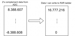


To convert Two's complement data into binary offset format, the MSB must simply be inverted,
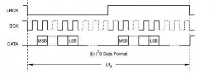
Another point to consider is that the I2S format transmits the LSB of the right/left channel after the WS has changed - so the MSB of the other channel is the second bit after the WS signal changed.
Another point to consider is that the I2S format transmits the LSB of the right/left channel after the WS has changed - so the MSB of the other channel is the second bit after the WS signal changed.
Another point to consider is that the I2S format transmits the LSB of the right/left channel after the WS has changed.
This is only partially correct. It only applies when the sub-frame length and the audio channel data length are the same as in the case of 16 bit words and 16 bit sub frames i.e. CLAB/SCK is 32Fs.
Thanks for the replies! The dataformat that the ADC sends out is like you both say, it starts sending it's data 1 BCLK delayed and then transmits 24 bits. But a single channel in the LRCLK period is 32 clks long, so there is plenty of time before the LRCK changes.
I tried implementing the simple solution that Aboos suggested with just inverting the first bit of the received data:

And it seems to work great in simulation:
With MSB set to 0:

With MSB set to 1:

But when I try the code on the FPGA with the R2R-ladder, it still sounds horrible :S I might have to resort to implementing an ILA core in my FPGA to have a look at the signals inside in real time.
Any Ideas are more than welcome 🙂
/Kenneth

I tried implementing the simple solution that Aboos suggested with just inverting the first bit of the received data:

And it seems to work great in simulation:
With MSB set to 0:

With MSB set to 1:

But when I try the code on the FPGA with the R2R-ladder, it still sounds horrible :S I might have to resort to implementing an ILA core in my FPGA to have a look at the signals inside in real time.
Any Ideas are more than welcome 🙂
/Kenneth
Having made the data serial you then have to align the active 24 bits with your ladder. That is easily done with a 64 bit shift register.
Step 1: test the R2R ladder.
Step 2: test you correctly decode an I2S known signal.
Step 3: combine the two.
Trying to debug the combined system just makes life harder.
BTW. R2R ladders deyond about 10 bits is unlikely to work any better than 10 bits with exception attention to resistor tolerances, supply voltage stability, switch elements, You aren't trying to use FPGA logic outputs directly without buffering?
I made one discrete DAC. Maybe it would be of help.
- The Latch enable = Word Clock have to be 32bit. 32 BCK Bit clock. All contemporary USB interfaces use the same word lenght 32bit. first 16 or 24 bits are datas other are "empty" zeroes. (except in case of 32 bit word...)
- R2R switching network can be from 16bits-24bits-32birs does not matter much but if You are not listening 32bit songs seems without the point spending money on not ceep precise R to fill up to 32bits and they aways be zeroes from LSB of 24bit word?
- Input format is NOT I2S but LEFT justified. That need to delay LE for ONE BCK. example from PMD100 datasheet page 17. one inverter and one Flip flop..
- MSB of the Left jusified format must be inverted
Okay update time
I've finally managed to get somewhat proper sound out of my setup now 🙂 I changed my R2R-ladder to a 16-bit configuration, because most of the internet (and here too) agreed that you would need ridiculously precise resistors to have a 24-bit R2R ladder make sense. I also added buffers on the drive pins out of the FPGA, even though my calculations said that the FPGA should have been more than capable of driving the ladder. Another reason I added the buffers was because some of the drive pins have in-line 220R resistors on the FPGA board, making the 3K/1.5K ladder become "unbalanced". I had originally figured that it would make little to no difference, but now with the buffers, I know that's not the issue 🙂
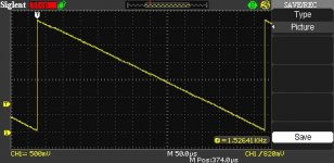
After the hardware change to 16-bit and with buffers, I ran a test on the R2R-Ladder with a simple counter in the FPGA and all looked good:
I changed the input gain of my PCM4220 ADC and I'm now able to get signal out of my R2R-ladder. I was probably driving the inputs at such a low level that I was basically just getting noise out. Im still using the code from before to invert the MSB, which seems to work, but I'm seeing a "jump" when crossing zero? (Sorry for bad picture, I didnt have a USB on me that day - Green is input and yellow is output):
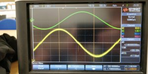
Any idea what might cause this jump?
/Kenneth
I've finally managed to get somewhat proper sound out of my setup now 🙂 I changed my R2R-ladder to a 16-bit configuration, because most of the internet (and here too) agreed that you would need ridiculously precise resistors to have a 24-bit R2R ladder make sense. I also added buffers on the drive pins out of the FPGA, even though my calculations said that the FPGA should have been more than capable of driving the ladder. Another reason I added the buffers was because some of the drive pins have in-line 220R resistors on the FPGA board, making the 3K/1.5K ladder become "unbalanced". I had originally figured that it would make little to no difference, but now with the buffers, I know that's not the issue 🙂
After the hardware change to 16-bit and with buffers, I ran a test on the R2R-Ladder with a simple counter in the FPGA and all looked good:

I changed the input gain of my PCM4220 ADC and I'm now able to get signal out of my R2R-ladder. I was probably driving the inputs at such a low level that I was basically just getting noise out. Im still using the code from before to invert the MSB, which seems to work, but I'm seeing a "jump" when crossing zero? (Sorry for bad picture, I didnt have a USB on me that day - Green is input and yellow is output):

Any idea what might cause this jump?
/Kenneth
I’m assuming the counter image is a simulation, and the sine wave is the system running. Do you see the same problem running the simulation on a sine wave? If you do, then I’d say you’ve got an off by one error somewhere in your code. If not, your code is probably good, but perhaps some of the resistors in your ladder are swapped?
Okay update time
Any idea what might cause this jump?
/Kenneth
When the digital signal crosses zero, the MSB bit switches, but all the other bits switches the other way. That is usually the worst case with a regular DAC as there is where the largest resistor mismatch happens, that's why most high end chips have an adjustment for the MSB bit, see t.ex. the AD1865 datasheet. The fix is to do a Sign Magnitude DAC, using two resistor networks....
You might want to read the dam1021 thread, plenty of info.
And I thought DA conversion was done using an array of switchable current sources feeding current into the same resistor. For instance, a 3 bit DA converter would use currents with these magnetudes: 8i, 4i and 2i (i is a constant).
I have a home-brewed algorithm for an n bit AD converter which uses a loop consisting of n iterations, one iteration per bit. It would work something like this:
I have a home-brewed algorithm for an n bit AD converter which uses a loop consisting of n iterations, one iteration per bit. It would work something like this:
Code:
01.  Initialise all bits to zero
02.  Enter loop.
03.  Set the most significant bit to 1.
04.  Convert this to its equivalent analogue signal and compare it with the signal to be converted.
05.  If converted signal is smaller than input signal, the bit is 1, otherwise, it is 0.
06.  Move to next bit.
07. Go to 02.There are many ways to convert digital signals into an analogue form and vice versa. See page 30 and beyond of this article for some early methods that have become unusual:
BSTJ 27: 1. January 1948: An Experimental Multichannel Pulse Code Modulation System of Toll Quality. (Meacham, L.A.; Peterson, E.) : Free Download, Borrow, and Streaming : Internet Archive
BSTJ 27: 1. January 1948: An Experimental Multichannel Pulse Code Modulation System of Toll Quality. (Meacham, L.A.; Peterson, E.) : Free Download, Borrow, and Streaming : Internet Archive
Any idea what might cause this jump?
/Kenneth
It is a "standard" binary code glitch during change of MSB against other bits has the same value. Because You use FPGA I think That You can identify state when it is happening and mute output with fast switch? Take a look at the circuits controled by the deglitch signal.
.
Other way is at analog side, to ad simple RC filter, but that will increase settling time and not clear the glitches 100% but decrese them significantly
link:https://www.edn.com/electronics-blogs/bakers-best/4368256/Use-an-RC-filter-to-deglitch-a-DAC
Attachments
When the digital signal crosses zero, the MSB bit switches, but all the other bits switches the other way. That is usually the worst case with a regular DAC as there is where the largest resistor mismatch happens, that's why most high end chips have an adjustment for the MSB bit, see t.ex. the AD1865 datasheet. The fix is to do a Sign Magnitude DAC, using two resistor networks....
You might want to read the dam1021 thread, plenty of info.
Actually, maybe the only fix for that, glitches, is to convert binary to grey code before conversion 🙂
When the digital signal crosses zero, the MSB bit switches, but all the other bits switches the other way. That is usually the worst case with a regular DAC as there is where the largest resistor mismatch happens.......
Yes yes! This makes perfect sense, right when crossing through zero, there would be the most amount of bits changing at the same time, making even a small change in resistor tolerance quite noticeable! The jump in the signal going through zero is around 20-30mV which is pretty high, but then again we did construct the R2R-ladder with 3K 1% and 1.5K 5% resistors, so those kind of numbers don't seem completely unreasonable.
Going into this project we knew that we were never gonna make a great sounding DAC, but it has been eyeopening just how much precision is required. As this is a school project and we have a pretty tight time frame, we are choosing to accept this "usable-but-not-great-sounding" implementation and move on with the rest of the project, where we implement a biquad filter, I2S receiver and R2R driver on an ZynQ board, where we can adjust the biquad parameters from the processor system on the ZynQ 🙂
Thanks to everyone helping out and replying, it really helped a lot with my understanding of the data being sent in an audio system, and the surprisingly difficult task of making a decent R2R DAC 😛
/Kenneth
- Home
- Source & Line
- Digital Line Level
- Making an I2S R2R DAC with a FPGA
