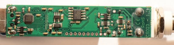
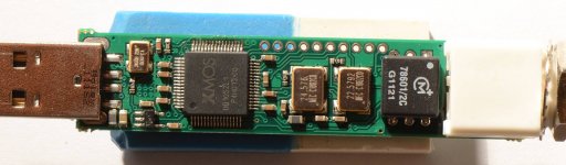
for everyone who is interested, a look inside M2TECH hiFace Two
fullres, cca 4500x1200 here:
http://netload.in/dateijQ68qYeHID/hiface2.zip.htm
Best Regards
;-)
fullres, cca 4500x1200 here:
http://netload.in/dateijQ68qYeHID/hiface2.zip.htm
Best Regards
;-)
Attachments
Last edited:
Thermal relief on some GND vias not others! Copper pours slivers with no via at one end, antennas. USB3318 thermal vias devoid of copper pour on bottom layer. A couple of dodgy looking solder joints and some flux not cleaned off. T juction traces near the xtals.Nothing special, standard commercial type basic layout a bit scrappy.
It looks like the connectors and through hole components have been soldered on after the SMD assembly, not the best joints I have seen.
If I was to categorize the quality of this assembly I would say it is lower end consumer products, IPC class 1 workmanship and general quality.
If I was to categorize the quality of this assembly I would say it is lower end consumer products, IPC class 1 workmanship and general quality.
🙂
I was being polite, as whenever I seem to open my mouth on here regarding PCB design, quality , workmanship or clock mods (the bodge ones involing 10s to 100s of MHz) I get shot down, often cos my views dont fit with the fantasy world of design some exist in.😀There from the real world...
I was being polite, as whenever I seem to open my mouth on here regarding PCB design, quality , workmanship or clock mods (the bodge ones involing 10s to 100s of MHz) I get shot down, often cos my views dont fit with the fantasy world of design some exist in.😀There from the real world...
- Status
- Not open for further replies.