Hi guys ,
I have been working on blameless design for quite some time , the problem I am facing is increased DC offset of around 70 to 140mV. With a tail current of approx 2mA I am getting a offset of around 140mV and if I drop the tail current to 1.2mA per device I get a offset of 70mV. I understand this is happening due mismatch of the LTP transistors Vbe and Hfe . Would it be advisable to use something like a MMDT5401 i.e dual matched PNP transistors in small SOT 363 package ?
Regards
It is probably not primarily due to mismatch of LTP transistors.
Virtually all amplifier designs have a systematic offset that is there even if all the pairs are perfectly matched. If you were to put your design in LTspice, that offset would show up, because LTspice assumes all transistors with the same model are perfectly matched. Paired transistors with different Vce adds offset. The error of having to feed base current asymmetrically adds offset. Have you simulated the circuit?
There are some highly matched devices available, of varying suitability depending on your supply voltage.
Can you post a picture of your schematic?
Are the DC resistances that both bases see the same? If not, you will get an offset that is proportional to the tail current even with perfect transistor matching.
If you’re getting 140 mV of offset just due to input bias current, you’ve got to be using some pretty low gain input transistors. It is more often caused by the demands of other things, such as VAS loading. If the VAS derives it’s input voltage from a resistor, perhaps that resistor needs to be trimmed to get good input balance. Even with perfectly matched transistors, if the input stage *currents* are not forced into balance you lose all the benefits of the matching of the transistors.
Put presets in the input stage, trim to get better results.
Resistors within 20 % tolerance are common, and the spec for electrolytic capacitors is 20% anyway, even for the best ones.
Use a scope if you have one.
Resistors within 20 % tolerance are common, and the spec for electrolytic capacitors is 20% anyway, even for the best ones.
Use a scope if you have one.
I am using 2N 5401 is the LTP and CCS and BC846 in theIf you’re getting 140 mV of offset just due to input bias current, you’ve got to be using some pretty low gain input transistors. It is more often caused by the demands of other things, such as VAS loading. If the VAS derives it’s input voltage from a resistor, perhaps that resistor needs to be trimmed to get good input balance. Even with perfectly matched transistors, if the input stage *currents* are not forced into balance you lose all the benefits of the matching of the transistors.
Current mirrors. I have tried both 2N5401 and KSA1381 in the VAS stages both seem to have similar offset .
Put presets in the input stage, trim to get better results.
Resistors within 20 % tolerance are common, and the spec for electrolytic capacitors is 20% anyway, even for the best ones.
Use a scope if you have one.
Hi Naresh , I don't use 20% resistor , it's all SMD 1% resistors
A leaking capacitor, or one polarity reversed if a polar electrolytic one, in the negative feedback shunt can cause an increased DC offset. Just a wild guess, but perhaps not impossible.
So if the input stage is 2n5401 with a beta of 100 (I think that is the beta for a 2n5401, could be wrong), and your collector current is 1.2ma, base current will be 12ua. If the input side of the LTP is say 47K to ground, and the feedback side of the LTP is 1K to ground, then roughly the input bias offset due to current is 46K x 12ua or 552mv. So base current can cause input offset voltages with different DC resistances to ground for the bias current. One of the reasons you want higher gain devices in the LTP and matching of the path to ground for the bias current.
It is probably not primarily due to mismatch of LTP transistors.
Virtually all amplifier designs have a systematic offset that is there even if all the pairs are perfectly matched. If you were to put your design in LTspice, that offset would show up, because LTspice assumes all transistors with the same model are perfectly matched. Paired transistors with different Vce adds offset. The error of having to feed base current asymmetrically adds offset. Have you simulated the circuit?
There are some highly matched devices available, of varying suitability depending on your supply voltage.
Can you post a picture of your schematic?
apologize for the delayed reply , please find attached schematic
Attachments
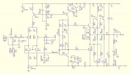
It looks like the winner is input resistor mismatch.
Left input transistor has a 26.3K resistance to ground.
Right input transistor has a 13K resistance to ground.
Input pair current looks like about 2.25mA each. 2N5401 can be low beta, but let's say it's 100. 22.5uA*13.3K = 300mV.
Quickest fix is to double the size of the feeback resistors, both Rseries and Rshunt. Harder fix is a bias servo.
Yes Russel , my first discrete amp.. I have worked on chip amps previously also designed some class D around IRS2092 and TAS5630...
Cool. That's a good first pick for an amp to build. What are the supply rails? I think some of the BC54x/BC55x series go up to 65V breakdown, and may work as a substitute for the input transistors.
I would play this one awhile, as is, get a feel for it's sound, and then begin making changes incrementally. Do the compensation cap reduction, if it can be done, then do the input pair. I don't know how flexible you are with doing schematic changes. Is this a PCB or did you hand-wire the whole thing? If the latter, you can try adding an EF buffer between the input pair and the VAS. That will increase linearity quite a lot.
Now you will want to invest in a USB 24-bit DAC/ADC, and some measurement software, like ARTA, so you can measure it's performance. Beware that voltage levels have to be attenuated to match the ADC's sweet spot, and not overdrive it.
What 24bit DAC would you suggest , I was looking at some Asus and creative sound cards and focusrite as input devices ...
I'm not really an expert on that. I'm thinking about getting the Quantalyzer QA-402 when they come out real soon now.
It needs to be 24-bit / 192 kHz of course. Play around over in the Equipment and Tools forum. There's tons of advice on which ones to use, and which DAC/ADC chips within them are the best. There's guys over there with auto-ranger input interfaces, that keep the ADC in its sweet spot without under or over-drive. Mostly.
I actually do not have an interface yet. I'm in the process of building up my lab from nothing, with a summer time-frame for purchase. I need everything: scopes, DMMs, power supplies, dummy loads, and an audio analyzer. I'm designing an amp right now, and I won't have that finished (the PCB) until this summer.
- Home
- Amplifiers
- Solid State
- LTP transistor Matching