I searched and didn't come up with much more than "it doesn't work". So I did some home work.
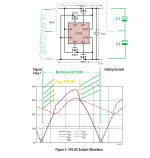
LT4320 is called something like an "ideal rectifier bridge controller". But the Figure 2 waveform in the datasheet shows it is a bit less than what you would call "ideal", in that the bottom FETs conduct over most of the input AC voltage cycle, much longer than the duration the top FETs conduct to charge up the output capacitor for.
Apparently such behavior results in the negative node of DC output gets tied to the bottom AC input node most of an AC cycle, and if we were to hook up a center-tapped transformer as well as the split-rail output capacitors, C1, C2, as we usually would to construct a full-wave split-rail PSU, the bottom capacitor C2 would be shorted out by the transformer windings through the bottom FETs during their extra conducting time period (hatched). This appears to be why "it doesn't work".
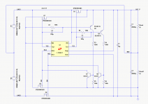
However, if we could somehow gate the bottom FET drives in such a way that they conduct and cutoff in sync with that of the top FETs', therefore, eliminating the extra conducting time, we probably could make it to work with a center-tapped transformer and be able to make a split-rail PSU with one LT4320.
I came up with a circuit as attached, for a 2 x 24 Vrms input. LTspice simulation indicates it would work just fine.
The 72V maximum voltage rating of LT4320 limits the use of the circuit to up to about +/-35V output. For higher output voltages we are out of luck but have to use two bridges and a transformer with fully separate output winding leads. Nevertheless for preamps and class A power amps that most likely operate under +/-35V, and especiall when having a center-tapped transformer flying around, this circuit perhaps is useful in either saving an expensive LT4320 and the four extra MOSFETs going with it or saving buying a expensive power transformer.
Attachments
If you need such discrete complication around the 4320 to end up being limited by voltage, why don't you take the plunge into full discrete: no more limitations, and you are not married to a specialty IC.
One or two sources for ideas, to brew your own, dedicated controller:
6.3 filament from 5vac winding
6.3vdc form 6.3v ac PSU
One or two sources for ideas, to brew your own, dedicated controller:
6.3 filament from 5vac winding
6.3vdc form 6.3v ac PSU
@ nattawa
Your great work a couple of years ago seems to have received much less attention than it deserves! Please receive my sincere thanks for the groud work you did!
Center tapped transformers are actually fairly wide spread in especially +/- 15V supply designs for OpAmp circuits, so it may be of value there, especially as several enthusiasts have had pleasing listening experience after changing away from Diode rectifiers in separate transformer sec. winding applications.
I do concede that the Diode Rectifier replacement with LT4320 circuits needs many more components and costs a lot more, but seems worthwhile for some. the opportunity shown to avoid transformer replacement and the second LT4320 circuitry should be of value.
Finally a question: Besides this simulation, have you physically built the circuit and tested it or revised it? ...or has anyone else done work on this alternative?
Kind Greetings,
Winfried
@ nattawa
Your great work a couple of years ago seems to have received much less attention than it deserves! Please receive my sincere thanks for the groud work you did!
……
Hi wgh52, I much appreciate your attention on my attempt of "abusing" the LT4320. Sorry for the late reply.
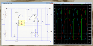
I didn't further the pursue by building an actual prototype, and I am glad I did not. The circuit seems to work fine in simulation when we look at its input and output voltages, yet by a closer inspection I discovered current spikes over the link that ties the center tap of the input and the center tap of the output. Under the load condition in the simulation, the current spike amplitude is abut 600mA, and it coincides with the top FET arm starts tuning on. It looks like this:
I did some further digging by reducing the circuit to different levels.
A) Straight diode bridge made with body diodes of the MOSFETs. MOSFETs stay shutoff. LT4320 out. There is no current spikes.
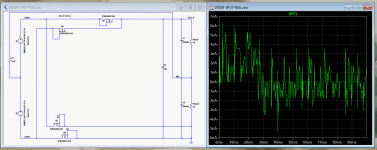
B) again straight diode bridge made with body diodes of the MOSFETs. NOSFETs stay shutoff. LT4320 in circuit but idling, not driving the MOSFETs. There are currents going on the GND link.... I don't like that
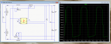
C) Top arm MOSFETs driven by LT4320, bottom arms remain normal diode connection with MOSFETs stay shutoff. We are seeing the spike GND currents.
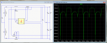
It appears the GND current spikes have nothing to do with the additional circuit I put in trying to sync up the top and bottom arm MOSFET gate controls, but instead are much related to LT4320's behavior under certain unintended "abuse" condition.
There could be chances that such behavior is an artifact due to the way the LT4320 Spice model being built without our way of "abusing" in mind. But so far I have had no means to prove it or otherwise. So at present I'd recommend against using the LT4320 the way I attempted.
