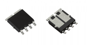
SQJ500AEP Dual complementary MOSFET from Vishay
I just came across this while looking for a low threshold/ logic level complementary pair. Does anyone have any experience with these? What did you think?
40V, 30A, 48W. They look good on paper, but I have questions. Like how much power can an SO8 package be reasonably expected to handle under real life conditions? What kind of heatsink does one use? The datasheet says 85 deg C /W when mounted on 1" sq. FR4 PCB. I wouldn't be comfortable dissipating more than 1 W from the pair. 😕
Any recommendations for a low threshold/ logic level complementary pair? High current, high power; not necessarily high voltage - even 5-12V will do.
Attachments
1W of dissipation from the pair (500mW each) will raise the 85C/W PCB traces by 85Cdegrees.
If the interior of the enclosure has a Ta=40degrees C, then the Tc of the devices are at ~ 125degreesC.
Now derate for elevated Tc and you don't have 40W devices, more like 8W
That leaves 7.5W per device for amplifying duty while the Tj=150degreesC.
I doubt it will last long.
If your Ta=50degreesC?
Now do the arithmetic for a 20C/W shared between the two devices.
Last edited:
Actually, just 2W total will raise the junction temperature by 170 deg C. The maximum allowed is 175 deg C. I wouldn't exceed 1W total, ever, unless we can find some PCB material with very good thermal conductivity. This device might have some use in low power applications, but I'm giving up on it for power amp use.
Sigh. Back to a hunt for discrete devices. What do you use for complementary pairs with low Vgth that can be fully driven with gate drive under 5V?
Sigh. Back to a hunt for discrete devices. What do you use for complementary pairs with low Vgth that can be fully driven with gate drive under 5V?
All you have to do is get creative with your thermal solution. Flip the devices upsidedown down so the thermal pads are top side. Mount them on the side of the PCB that has no other, or only low height, components and add a heatsink plus interface material.
I like the way you think. What are your sugestions for the connections? Is it OK to bend the leads of SO-8 packages? I've done that with DIP (way back when I messed up the PCB design and got mirror image PCBs), but not for any SMD.All you have to do is get creative with your thermal solution. Flip the devices upsidedown down so the thermal pads are top side. Mount them on the side of the PCB that has no other, or only low height, components and add a heatsink plus interface material.
It's not OK, it's very easy to crack the case because the leads are very hard after they press the shape into the copper. The leads on those miniature packages are so close to the board that you could still solder it straight on (reliability issues be damned)
Alternatively you can get a reasonably good amount of thermal conductance with thin PCB and a thermal via array. You can then attach the heat sink onto the other side of the PCB which is much simpler.
You will still have a challenging time reaching more than about ~3W dissipation out of a single SO-8 package.
Finally the elephant in the room with dual complementary MOSFET's intended for switching applications is that they're not actually anywhere near matched in linear conditions, so having them in the same package is really quite pointless as the thermal matching doesn't do anything useful for you.
Thanks, mt490. I thought as much. 🙁
Sigh. Back to a hunt for discrete devices. What do you use for complementary pairs with low Vgth that can be fully driven with gate drive under 5V?
Sigh. Back to a hunt for discrete devices. What do you use for complementary pairs with low Vgth that can be fully driven with gate drive under 5V?
- Status
- Not open for further replies.
- Home
- Amplifiers
- Solid State
- Low threshold/ logic level MOSFET Complementary Pair