Yes, understood. As I mentioned in #11, the s/n at C4, or the collector of Q2 is not bad -- around -60db. But ends up probably -40db or worse by the end.If Q1 is generating hiss you will find the level alters as you alter the volume VR1. If you have hiss with the volume on minimum then its coming from a later stage. Each stage runs at high gain and so all the effects are cumulative.
This is definitely a good ideaThe carbon comp resistors could be an issue. Obvious ones to swap out would be those in the bias networks to all the transistors.
btw, theses RCA transistors with integrated heatsink (40409/10?) were common in the early 70s
Last edited:
They look it. It's hard to believe modern transistors would not be much quieter...btw, theses RCA transistors with integrated heatsink (40409/10?) were common in the early 70s
Humor me for a moment: let's say I put a JFET in there per @MarcelvdG suggestion.
If noise is expressed in nv/√ hz for these Q1 components, and the existing one is about 4 and the JFET is less than 1; is there a way to calculate how much difference that would make in signal to noise in that circuit?
Lol, that's above my paygrade 😉
Have a play with this:
https://keith-snook.info/calculators/CC-Amplifier-noise.html
For Q1 I got this.

Have a play with this:
https://keith-snook.info/calculators/CC-Amplifier-noise.html
For Q1 I got this.

Nice!! Much closer to your paygrade than mine. I'm not sure of all the numbers to punch in but I'll try to figure it out.Lol, that's above my paygrade 😉
Have a play with this:
https://keith-snook.info/calculators/CC-Amplifier-noise.html
For Q1 I got this.
But interesting because that figure 53db sounds right about bang on, maybe a bit worse for good measure.
You can represent the noise of a three-terminal amplifying device such as a bipolar transistor or a JFET with two equivalent input noise sources, one noise voltage source and one noise current source. You can compare their effects on the total noise when you know the impedance that drives the input (base, gate, grid); for example, when the driving impedance is 50 kohm, 1 pA/√Hz has as much effect as 50 nV/√Hz.
The impedance of an electric guitar is very inductive, hence it is low at low frequencies, but hundreds of kiloohm at high audio frequencies. Besides, you have 47 kohm (originally even 120 kohm) resistors in series. Hence, the impedance is 47 kohm at low frequencies and a lot more at high audio frequencies.
Q1 is biased at just below 1 mA. The current gain of the original transistor is about 300, so its base current is about 3 uA. A current of 3 uA through a semiconductor junction produces a shot noise of about 1 pA/√Hz, and some extra 1/f noise that depends on how well the transistor was made and whether its base-emitter junction ever got damaged by reverse breakdown. That 1 pA/√Hz contributes to the equivalent input noise current and has as much impact as 47 nV/√Hz ... hundreds of nV/√Hz of noise voltage would have had.
As long as you bias it normally, a JFET has practically no gate current and almost no equivalent input noise current. Whether its equivalent input noise voltage is 1, 4 or 10 nV/√Hz doesn't matter much, because the series resistor at the input produces almost 30 nV/√Hz of its own.
For the record, using a JFET was bucks bunny's idea, I just agree it makes sense.
You can represent the noise of a three-terminal amplifying device such as a bipolar transistor or a JFET with two equivalent input noise sources, one noise voltage source and one noise current source. You can compare their effects on the total noise when you know the impedance that drives the input (base, gate, grid); for example, when the driving impedance is 50 kohm, 1 pA/√Hz has as much effect as 50 nV/√Hz.
The impedance of an electric guitar is very inductive, hence it is low at low frequencies, but hundreds of kiloohm at high audio frequencies. Besides, you have 47 kohm (originally even 120 kohm) resistors in series. Hence, the impedance is 47 kohm at low frequencies and a lot more at high audio frequencies.
Q1 is biased at just below 1 mA. The current gain of the original transistor is about 300, so its base current is about 3 uA. A current of 3 uA through a semiconductor junction produces a shot noise of about 1 pA/√Hz, and some extra 1/f noise that depends on how well the transistor was made and whether its base-emitter junction ever got damaged by reverse breakdown. That 1 pA/√Hz contributes to the equivalent input noise current and has as much impact as 47 nV/√Hz ... hundreds of nV/√Hz of noise voltage would have had.
As long as you bias it normally, a JFET has practically no gate current and almost no equivalent input noise current. Whether its equivalent input noise voltage is 1, 4 or 10 nV/√Hz doesn't matter much, because the series resistor at the input produces almost 30 nV/√Hz of its own.
For the record, using a JFET was bucks bunny's idea, I just agree it makes sense.
Thanks so much, man. I'm getting a good education in solid-state electronics. 😎 I think I see what you're saying, that the transistor is not so much the source of the noise. I only changed one of the input resistors, putting 47K in parallel to R2 for 33k. Should I do both, or go even lower? I put a 10k input (from 68K) on my Fender tube amp. With guitar amps, it's hard to get sound in the 2k-7k Hz "treble" range without a lot of noise. This amp has a surprising amount of noise at low frequencies too.
I'm going to try the JFET just for the hell of it - have to make a mouser order anyway.
From the specifications you provided ( IDSS of at least 2 mA and breakdown voltages over 30 V), I think this looks like the best match (?) on Mouser; https://www.mouser.com/ProductDetail/Linear-Integrated-Systems/LSK170B-TO-92-3L-BK?qs=T%2BzbugeAwjjZsjTzJGs9IA== There are others in that range that don't match the form factor of the original BJT. Does this look good?
Last edited:
Two line summary of my previous post: the noise associated with the base current of the transistor is the main noise source, hence a device without base current, such as a JFET, would be better. The noise voltage of just about any JFET will be far from dominant.
I only changed one of the input resistors, putting 47K in parallel to R2 for 33k. Should I do both, or go even lower? I put a 10k input (from 68K) on my Fender tube amp. With guitar amps, it's hard to get sound in the 2k-7k Hz "treble" range without a lot of noise. This amp has a surprising amount of noise at low frequencies too.
Assuming you use only one input, reducing the series resistor of that input further will help to reduce the input stage noise. In general, for low noise, any resistor in series with the signal source should have a small value and any resistor in parallel with the signal source should have a large value.
I don't know what the practical limit is. If the resistor is also meant to protect the input stage against excessive input signals, then reducing its value will reduce that protection.
Probably needless to say, but any change to the input stage will not help against the noise that remains when VR1 is turned fully anticlockwise/counterclockwise.
From the specifications you provided ( IDSS of at least 2 mA and breakdown voltages over 30 V), I think this looks like the best match (?) on Mouser; https://www.mouser.com/ProductDetail/Linear-Integrated-Systems/LSK170B-TO-92-3L-BK?qs=T%2BzbugeAwjjZsjTzJGs9IA== There are others in that range that don't match the form factor of the original BJT. Does this look good?
Yes, that should work fine, as should many other types.
It may be a good idea to add a 1N4148 to protect against excessive negative input voltage peaks (the JFET's gate-source junction will protect it against positive peaks). Cathode to the gate of the JFET, anode to ground.
Cool thank you. Ordering that now. Will post results when I try that.It may be a good idea to add a 1N4148 to protect against excessive negative input voltage peaks (the JFET's gate-source junction will protect it against positive peaks). Cathode to the gate of the JFET, anode to ground.
On guitar amps, the input grid stopper resistors are supposed to help block radio frequency noise, as I understand it. So with no resistor there at all (which I have tried on my other amp), you can get radio interference.
I have put a resistor there in parallel rather than swapping it out because the 45 year old PCB board is very prone to lifted traces, so I want to keep it original and undamaged as much as possible.
Update here:Replacing an NPN with an N-channel JFET usually requires a bias circuit redesign, but in the case of Q1, it doesn't. Just check what N-channel JFETs in a suitable package with an IDSS of at least 2 mA and breakdown voltages over 30 V are still available, buy one and connect it there, drain to where the collector used to be, gate to base, source to emitter. Whether it is useful to try this depends on the outcome of the VR1 experiment.
I installed an LSK170 JFET in place of Q1 as described above.
It is definitely lower noise, and also maybe higher gain, which is a good thing!!
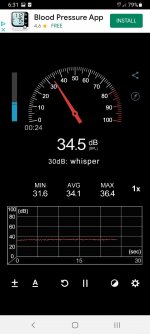
This is my quasi-scientific measurement with the noise meter app, right at the speaker grille, all knobs on 10 -- before/after.
Thank you so much for the advice and feedback on this - I'm so glad I asked, this really improved the amp for sure. 🙏 🙏 🙏 🙏
One more question if anyone wants to indulge me: What are the tone capacitors that could be changed in the tone stack here? I saw a post by a Japanese guy who modified the "treble coupling cap" (which one is that?) and the mid resistor. Link here, google translate. http://prosoundsos.jugem.jp/?eid=97
The way the amp's tone sounds now, I almost can't turn the bass down enough, and it is lacking highs. Sounds great now, though.
Attachments

Last edited:
I'm glad @bucks bunny 's proposal worked out well!
C6, C7 (bass), C8 and C9 (treble) are the main tone control capacitors, and R12, R13, R14 and the treble and bass potmeters are the tone control resistors. Shorting or reducing R13 should allow you to reduce the bass further, increasing C8 to further increase treble. I wonder if there is anything wrong with any of those components, as the bass and treble control ranges should be pretty large by design.
Increasing R3 to 1 Mohm or 2.2 Mohm should also improve treble if you have a very inductive guitar pick-up.
BTW -- Is the idea of this diode to deal with DC voltage on the input? Because I'm getting a scratchiness when I turn the guitar's volume pot now that the JFET is in there (it's not a problem with the guitar's pot). I read only about 10-15mv of DC on the input (guitar cord). Is there a better way to deal with this?It may be a good idea to add a 1N4148 to protect against excessive negative input voltage peaks (the JFET's gate-source junction will protect it against positive peaks). Cathode to the gate of the JFET, anode to ground.
You're saying that diode should go from JFET gate to ground, not in series with the gate where it replaces the transistor?
I meant this, apologies for the rotated picture. The only purpose of the extra diode from the gate to ground is to protect the JFET against excessive input signals (due to electrostatic discharge, or the wrong plug being plugged into the input by mistake, whatever).

Thanks very much for that. I have that diode and will put it in.I meant this, apologies for the rotated picture. The only purpose of the extra diode from the gate to ground is to protect the JFET against excessive input signals (due to electrostatic discharge, or the wrong plug being plugged into the input by mistake, whatever).
For the DC on the input, could you suggest a value and placement of a coupling cap to deal with that? I tried a .1uf directly before the input hot lead and it seemed to work, but I'm not sure.
C1 is supposed to keep DC from the input, but if it has a 470 Mohm leakage resistance, you already get 13 mV of residual DC voltage with open input.
If C1 is the original electrolytic capacitor, you can leave the amplifier on for an hour or two to see if C1's dielectric reforms and the DC at the input drops, or replace it with a newer capacitor, preferably a film capacitor if that fits.
If you get results that make no sense at all, the scratchiness could also be due to parasitic oscillations, although I would not expect that; R1 or R2 should prevent it.
Last edited:
You might also get some DC current leaking into the input if the PCB is dirty between the pins of C1 or between any node biased at a substantial voltage and the input. Flux residues and some moisture form an electrolytic conductor, for example.
Ah so, thanks. Yes, the DC on the input gradually subsides, starting at about 3v DC last I checked. However this is an issue only since putting in the JFET (which is overall a great improvement), so the JFET must be in some way leaking DC to the input (?) I'm looking for some way to work around that.C1 is supposed to keep DC from the input, but if it has a 470 Mohm leakage resistance, you already get 13 mV of residual DC voltage with open input.
If C1 is the original electrolytic capacitor, you can leave the amplifier on for an hour or two to see if C1's dielectric reforms and the DC at the input drops, or replace it with a newer capacitor, preferably a film capacitor if that fits.
If you get results that make no sense at all, the scratchiness could also be due to parasitic oscillations, although I would not expect that; R1 or R2 should prevent it.
Also still unable to resolve hum on reverb circuit somewhere in Q5 area, but that's another story.
What time does it take for the voltage to drop from 3 V to 15 mV? Of the order of four seconds or much longer than that?
If it is some oscillation issue after all, then a 47 ohm resistor (or anything from 47 ohm to 220 ohm) between the gate and everything else, placed as close to the gate as possible, could help. Something like this, please ignore the gaps in the wires:

If it is some oscillation issue after all, then a 47 ohm resistor (or anything from 47 ohm to 220 ohm) between the gate and everything else, placed as close to the gate as possible, could help. Something like this, please ignore the gaps in the wires:
Last edited:
- Home
- Design & Build
- Parts
- Low-noise equivalents for BC169B and 2N4062 transistors