Hi all,
Please feel free to use this thread for everything related to your ES9018K2M dac build. Ask questions, seek advice, and share tips, techniques, and photos.
Regards.
Please feel free to use this thread for everything related to your ES9018K2M dac build. Ask questions, seek advice, and share tips, techniques, and photos.
Regards.
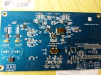
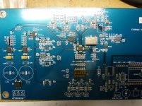
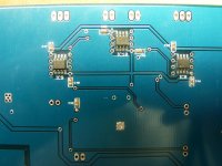
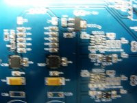
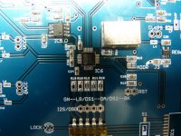
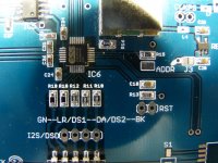
Started soldering today. My plan is to leave off mcu etc. and use dac in default mode at first. everything in lower right will not be populated. Im using the SOIC opamps and the ADP151 regs. My only question so far is what to do with the ADDR pads. Let me know if you see anything amiss.
Thanks. Cheers.
Thanks. Cheers.
Attachments
I will use separate 5V power supply and not derived from V+ .
A superreg that will provide +5V and will not solder REG2 .
Also the transformer will have separate secondary at about 10V ac with separate diode and capacitors for this .
And a silver mica capacitor of 1nF in position of C12.
A superreg that will provide +5V and will not solder REG2 .
Also the transformer will have separate secondary at about 10V ac with separate diode and capacitors for this .
And a silver mica capacitor of 1nF in position of C12.
I will use separate 5V power supply and not derived from V+ .
A superreg that will provide +5V and will not solder REG2 .
Also the transformer will have separate secondary at about 10V ac with separate diode and capacitors for this .
And a silver mica capacitor of 1nF in position of C12.
Hi,
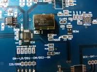
Do you mean to leave out REG2 and use separate superreg with separate winding from the transformer for feeding the DC-5V (circule in red) ?

The 5V is about 100mA, and the 3.3V, 300mA....maybe excessively high but not much excessive!
Some shuntreg can provide 400mA...but the really critical voltage is buffered in the circuit by the lm4562 in follower configuration!
The schematic provide by Syllabe show a smart implementation of the DAC.
Some shuntreg can provide 400mA...but the really critical voltage is buffered in the circuit by the lm4562 in follower configuration!
The schematic provide by Syllabe show a smart implementation of the DAC.
But where did you get these numbers from? Do you have the ES90182KM datasheet?
We're powering the DAC chip, the clock and the possibly an spdif input buffer. These are all 3.3V, so what's the 5V powering? The MCU comes from a different supply.'
Thanks.
We're powering the DAC chip, the clock and the possibly an spdif input buffer. These are all 3.3V, so what's the 5V powering? The MCU comes from a different supply.'
Thanks.
Yes, you're right!
..I say 100mA for 5V for the Clock, which is 3.3V supply and has 40mA consumption in idle ...taking 100% marge of comsumption, 100mA... and 300mA, for the DAC itself, one more time, more than double of the real consumption!
..I say 100mA for 5V for the Clock, which is 3.3V supply and has 40mA consumption in idle ...taking 100% marge of comsumption, 100mA... and 300mA, for the DAC itself, one more time, more than double of the real consumption!
Hi everyone,
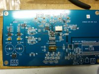
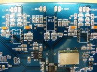
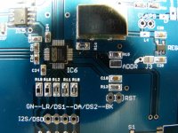
The build continues. I think I have all SMD components mounted except for the ferrites. The jumpers are still open as well. My plan is to verify voltages and then gradually connect jumpers and beads. Let me know if there is a checklist I should follow. Please let me know if you see anything amiss. Thanks so much.
The build continues. I think I have all SMD components mounted except for the ferrites. The jumpers are still open as well. My plan is to verify voltages and then gradually connect jumpers and beads. Let me know if there is a checklist I should follow. Please let me know if you see anything amiss. Thanks so much.
Attachments
-
 P1030827.jpg992.7 KB · Views: 1,123
 -
 P1030828.jpg995.5 KB · Views: 927
 -
 P1030829.jpg853.1 KB · Views: 833
 -
 P1030830.jpg908.9 KB · Views: 795
 -
 P1030831.jpg981.7 KB · Views: 755
 -
 P1030832.jpg980.1 KB · Views: 240
 -
 P1030833.jpg986.1 KB · Views: 221
 -
 P1030834.jpg972.8 KB · Views: 256
 -
 P1030835.jpg920.8 KB · Views: 290
Hi,
Do you mean to leave out REG2 and use separate superreg with separate winding from the transformer for feeding the DC-5V (circule in red) ?
[/URL][/IMG]
Yes .
Ok in the range of 300mA ...350mA...400mA .
No shunt . I think you cannot do better sound to put shunt in this position
Better a classical lm723 with BD series like Subbu do on his DAC.
Or for the hurry ones a 5V low noise like LT17635 , very good for this position .
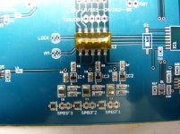
ADDR is the chip address. In stand alone, without MCU, we don't care about his value.
The ADDR pads appear to be a jumper. Should I close it if not using mcu?
The ADDR pads is a jumper indeed!
If you close it, the chip adress will be 0x90, if you don't, the 0x92. In all case, without MCU, the DAC always works. You can closed or let it opened!
The adress pin is used to distinguish chip in mono use!
If you close it, the chip adress will be 0x90, if you don't, the 0x92. In all case, without MCU, the DAC always works. You can closed or let it opened!
The adress pin is used to distinguish chip in mono use!
- Status
- Not open for further replies.
- Home
- Source & Line
- Digital Line Level
- Low cost ES9018 Dac - Builders Thread