Hey guys, I've got a couple Bode plots for you to look at. I'm a bit puzzled by this and hope you can help me sort things out.
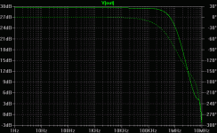
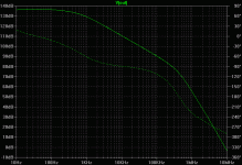
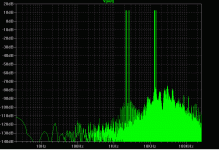
First, open loop. Then, closed.
In simulations, the closed loop is stable, even with 1uF capacitive load. Step response is smooth, no overshoot. The implication would be stability.
But looking at the amplitude and phase, it seems that there's way too much phase to allow the loop to be closed and remain stable. The closed loop is stabilized with the addition of between .68pF and 1.5pF across the FB resistor (301K Ohm).
What am I missing with gain and phase margin here?
Last edited:
maybe it's just a minus sign, but at low frequencies, the phase is 0 degrees, not -180.
Can you post the schematic?
Can you post the schematic?
If you look more closely, you'll see the phase is zero at low frequencies. It reaches 180 degrees at around 600KHz in the open loop plot.
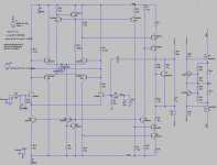
The schematic is rather cumbersome. But I'll try and clean it up and post a partial.
One correction. The 1pF cap is from the drive to the MOSFETS, not directly across the FB resistor.
The schematic is rather cumbersome. But I'll try and clean it up and post a partial.
One correction. The 1pF cap is from the drive to the MOSFETS, not directly across the FB resistor.
The zero phase at low frequencies is what has me going...doesn't that say that it's positive feedback at low frequencies, which means it would latch up at DC?
That's why a look at the schematic might reveal the mystery, I hope.
Is it in LTSpice? If so, could you post your .asc file?
That's why a look at the schematic might reveal the mystery, I hope.
Is it in LTSpice? If so, could you post your .asc file?
It's a non-inverting amp. That's why at low frequencies the phase is zero. It's in phase with the input.
Here's a shot of the schematic. There are a few more MOSFET sections.
It's a JFet differential input which drives a complimentary differential pair. All three of those are fed with current sources. The complimentary pairs are also loaded with current mirrors which function as the drive signals for the MJE340 and 350.
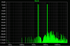
The modeled performance is pretty dang good too. Here's a shot of a simulation using a signal with a 10:1 crest factor (music facsimile) using 10 tones in two closely spaced groups to highlight IMD performance. 60V peaks into 8 Ohm. It stays virtually identical when loaded with 4 Ohm.
For the Bode Plots, I removed the input capacitor so that the plots showed only the amp itself. The 1uF cap at the output has a series resistance of 1K, basically out of the circuit.


Here's a shot of the schematic. There are a few more MOSFET sections.
It's a JFet differential input which drives a complimentary differential pair. All three of those are fed with current sources. The complimentary pairs are also loaded with current mirrors which function as the drive signals for the MJE340 and 350.
The modeled performance is pretty dang good too. Here's a shot of a simulation using a signal with a 10:1 crest factor (music facsimile) using 10 tones in two closely spaced groups to highlight IMD performance. 60V peaks into 8 Ohm. It stays virtually identical when loaded with 4 Ohm.
For the Bode Plots, I removed the input capacitor so that the plots showed only the amp itself. The 1uF cap at the output has a series resistance of 1K, basically out of the circuit.
Last edited:
Maybe this explains it? The phase shift where the 1pF cap is taking its feedback is lower than the overall phase shift and that's what gives the phase margin for stability?
It's been a while since my days of loop stability analysis. I can feel the rust breaking off the cogs upstairs.
It's been a while since my days of loop stability analysis. I can feel the rust breaking off the cogs upstairs.
Pete,
I think that your loop gain measurement methodology might be suspect. It's typically done by putting a source in that isn't the input.
In your circuit, you'd drop an AC source between the R3-R5 junction and the gate of J2. The loop gain is then the ratio of the R3-R5 voltage to the voltage at J2's gate. Maybe you made the measurement like that, but it's hard for me to tell without being able to see the source.
This is also one of those front ends that makes me worry owing to two dueling high gain stages. The Q-point is kind of fuzzy...easy way to see that would be to add 1 mV of offset to one transistor in the input stages, and see how much the current in the VAS changes.
Catch you tomorrow!
Your simulation parameters are too minimalistic. Since LTSpice is optimized for logic and switching, it comes default with data compression and low accuracy settings. Add these parameters to your schematic and see what happens:
.options plotwinsize=0
.options method=gear
.options numdgt=7
Also try removing C2 and see if it's still stable. Or give C2 some ESL.
To get a lower noise floor, select the Hann or Blackman window in the FFT dialogue.
I like R19 and R14. If the Hfe of the VAS can be counted on, bias may be stable. It would be interesting to see the influence of temperature and various things in the real prototype. Cascoding would make Hfe more stable.
If the output is shorted, which will fry first, Q7 or Q2?
Last edited:
adding a fet front end doesn't fix the Slone complementary diff pair + current mirror indeterminate VAS bias problem - you really need to understand the issue and fix it up before wasting time simming something that won't work with real components
Your simulation parameters are too minimalistic. Since LTSpice is optimized for logic and switching, it comes default with data compression and low accuracy settings. Add these parameters to your schematic and see what happens:
.options plotwinsize=0
.options method=gear
.options numdgt=7
Also try removing C2 and see if it's still stable. Or give C2 some ESL.
To get a lower noise floor, select the Hann or Blackman window in the FFT dialogue.
I like R19 and R14. If the Hfe of the VAS can be counted on, bias may be stable. It would be interesting to see the influence of temperature and various things in the real prototype. Cascoding would make Hfe more stable.
If the output is shorted, which will fry first, Q7 or Q2?
Thanks for the suggestions.
I had already removed compression and set the time step to 1us. But I did add your directives and re-ran the sims on both the closed loop gain and the 10 tone signal. Hann window on the FFT.
Maybe you missed my comment earlier. C2 has a 1000 Ohm series resistance for the simulations. It's hanging there so that it's easy to change and check stability with capacitive loads.
Q2 and Q7 are separated by a couple hundred ohms which limits the current to about 120ma peaks. Output current will be set to about 15A peak at which point the power supply fuse should have easily blown. We'll see if it's adequate or other protection needs to be added.
Input for the simulation is sent to the "Source" input of the dependent source on R2. The 30dB gain is set by the ratio of 301K / 10K. The 68pF cap was removed for the simulations to see the entire loop character without the LPF at the input.
R19 and R14: they will be set during testing to fix the bias current in VAS to somewhere between 20 and 30mA. I also have R9 and R10 so that I can further stabilize the drive transistors if need be. R7 and R8 also help bring a determinate state to the current mirror output levels. They can be modified to help set bias as well.
The JFet front end is not there to "fix" anything about the Slone pair or indeterminate VAS. The JFET front end adds a bit of gain and gives me the high input impedance I was after. It's also a low noise, matched pair, which doesn't hurt either (Linear Integrated Systems LS844). Besides, I can always remove the mirrors and replace them with fixed resistors and set the VAS bias that way, but it will give away a few dB of gain.
But back to the original point about phase shift and loop stability . . .
Attachments
Cascoding would make Hfe more stable.
Are you referring to adding a cascode stage to handle the voltage swing and keep Q2,8 at low voltage?
GIGO
you'd best do that now - before wasting more sim cycles
and wasting other poster's time time trying help when the basic circuit topology doesn't work reliably
Besides, I can always remove the mirrors and replace them with fixed resistors and set the VAS bias that way, but it will give away a few dB of gain.
you'd best do that now - before wasting more sim cycles
and wasting other poster's time time trying help when the basic circuit topology doesn't work reliably
you'd best do that now - before wasting more sim cycles
and wasting other poster's time time trying help when the basic circuit topology doesn't work reliably
How about contributing to the question at hand instead?
What can we gain from looking at the Bode Plots on loop stability?
I'll work on the actual circuit soon enough and find out what will and will not actually work with real parts on a real circuit card. The whole point of my post was not to critique the design, but to understand the Bode Plots and their relationship to loop stability.
There are some compensation configurations that make the loopgain plots confusing. For instance I had an amp that caused phase to wrap around the plot. I'm not exactly sure what's wrong in your case but since I can't tell from the schematic how you're deriving loop gain, I suggest you might be doing it wrong like djoffe says. Look in the /example/loopgain2.asc file in the LTSpice directory and use that method.
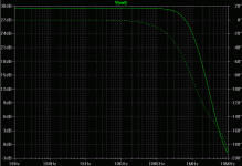
OK, I updated the schematic and removed the mirrors and added the cascode stage for VAS. The cascode is biased by a current source to maybe 3V from the rail. I ran new simulations on open and closed loop and got the Bode plots. Same questions still.
What on the plots reveals loop stability/instability?
BTW, the cascode stage using the 2N5551 and 2N5401 for gain and the MJE340 and MJE350 for the swing voltage added more than enough gain for what was lost by removing the mirrors. VAS bias current is set to 20mA with this setup.
What on the plots reveals loop stability/instability?
BTW, the cascode stage using the 2N5551 and 2N5401 for gain and the MJE340 and MJE350 for the swing voltage added more than enough gain for what was lost by removing the mirrors. VAS bias current is set to 20mA with this setup.
Attachments
There are some compensation configurations that make the loopgain plots confusing. For instance I had an amp that caused phase to wrap around the plot. I'm not exactly sure what's wrong in your case but since I can't tell from the schematic how you're deriving loop gain, I suggest you might be doing it wrong like djoffe says. Look in the /example/loopgain2.asc file in the LTSpice directory and use that method.
To generate loop gain, I put a 1F capacitor at the (-) input to ground to basically short it out without removing the DC portion.
I'll check out their suggested method and see if it does anything different.
post the .asc? - now an allowed forum file attachment type - I put any non-standard Q .model defs directly on the schematic for portability
The circuit looks unrealistic to me. You really expect to use a 1pF compensation capacitor? That is probably less than circuit stray capacitance. 301k for the feedback resistor? This is 10 times more than usual. No LTP emitter resistors? The theoretical extra loop return ratio is impractical I think.
David Zan
David Zan
post the .asc? - now an allowed forum file attachment type - I put any non-standard Q .model defs directly on the schematic for portability
I'm using Cordell's models for all the devices in the schematic.
I also derived the open loop gain by simply dividing the output by the difference between the (+) and (-) inputs at the JFET gates. I get the same thing by shorting the (-) input with a 1F capacitor. The open loop gain plot I posted is no different than the actual method for determining open loop gain, Vout/(V(+) - V(-)).
Attachments
The circuit looks unrealistic to me. You really expect to use a 1pF compensation capacitor? That is probably less than circuit stray capacitance. 301k for the feedback resistor? This is 10 times more than usual. No LTP emitter resistors? The theoretical extra loop return ratio is impractical I think.
David Zan
Hi David,
As for LTP resistors, I've put them in, and taken them out. 100 Ohm was the value I originally tried, and with this particular circuit, they didn't seem to make much difference one way or the other, either in open loop gain or closed loop gain or performance in general. Cleaner schematic without them.
As for compensation capacitance, who knows what it will actually be once the circuit is laid out and soldered up. For simulations, that's what worked.
301K feedback resistor with a JFet device is quite reasonable. If I do reduce it to 30.1K and the 10K to 1K, then the 1pF compensation moves to 10pF to keep everything on the bode plots the same and producing stable output.
- Status
- Not open for further replies.
- Home
- Amplifiers
- Solid State
- Loop stability clarification . . .