Fred,
I agree with all your comments on power supply, but would add that it's not so much the voltage regulation which matters, but rather issues of output impedance and intermodulation behaviour as current variations cycle. I suspect one of the reasons Class A sounds so much better than MOST class ABs is because the current taken from the power supply is much more consistent; the problems with Class ABs are frequently hidden issues with power supply response.
On another note, that picture you inserted a couple posts back. Was that the 'Book Police', from Ray Bradbury's Fahrenheit 451? If so, a very, very apt comment!
Cheers,
Hugh
* try to set the night on fire!
Ray Bradbury's Fahrenheit 451
Starring Oskar Werner and Julie Christie, directed by François Truffaut! What more could one ask for all in one movie?
* that was for jocko who even made me read Morrison's poetry for which I retaliated by making him watch Oliver Stone's The Doors.
Be thankful you have never heard his Ray Manzarek imitation:
" Jim's still alive man.... he sent me a postcard from Paris man....."
Hey man........
Take your medicactions, and go to bed.
And none of that "calm, calculus of reason" crap either.
Jocko
Take your medicactions, and go to bed.
And none of that "calm, calculus of reason" crap either.
Jocko
Re: Correction to my earlier post
Andy,
Excellent, very clear reasoning. It is always nice to see that what you expected intuitively is borne out by rigorous analysis. Following your analysis we can safely say that the PS impact on the output can be calculated by first dividing the PS noise/ripple by the PSRR and then multiplying it with the closed loop gain, right?
I have one question: In the def section you defined PSRR as the opamp open loop gain for diff input signals over the opamp open loop gain for PS disturbances. This seems logical, but I haven't been able to find this definition anywhere. Do you have reference for this?
Jan Didden
andy_c said:Okay, I know this is an old thread 😉 . But after reading the article suggested by jcx titled "A General Relationship Between Amplifier Parameters, And Its Application to PSRR Improvement", I realized that my previous analysis was in error and figured out what the error was. To avoid confusing anyone who ends up reading this thread at a later time, I'll go through the whole thing, showing where my error was. I'll demonstrate that jcx's formula for referring the power supply disturbance to the non-inverting input of the op-amp is quite correct. I'll use the notation from the above mentioned article to do this. Part of the problem with my previous posts was not having found a formal mathematical definition of PSRR in relation to other op-amp gains. The above article has a rigorous formal definition and its application leads at once to the formula jcx used to reflect the power supply disturbance to the non-inverting input. So here goes.
The definitions are:
Vd = op-amp difference-mode input voltage (V_plus - V_minus)
Vo = op-amp output voltage
Vi = op-amp input voltage (at non-inverting input)
Vcm = op-amp common-mode input voltage (I'll neglect it)
Ad = open-loop gain from op-amp differential input to output
Add = open-loop gain from op-amp positive supply to output
*** = open-loop gain from op-amp negative supply to output 😉
Acm = open-loop common-mode gain from op-amp input to output
Vdd = power supply disturbance at positive supply
Vss = power supply disturbance at negative supply (I'll neglect it)
PSRR_plus = power supply rejection ratio of positive supply
PSRR_plus = Ad / Add
B = feedback factor established by resistors/caps in feedback loop
From the above article:
Vo = Ad * Vd + Acm * Vcm + Add * Vdd + *** * Vss
Neglecting Vcm and and Vss, we get:
Vo = Ad * Vd + Add * Vdd
Since:
Vd = Vi - B * Vo
we have:
Vo = Ad * (Vi - B * Vo) + Add * Vdd
Setting Vi = 0 gives the output voltage due to a disturbance on the positive supply with no input voltage:
Vo * (1 + Ad * B) = Add * Vdd
or
Vo = Vdd * Add / (1 + Ad * B) (Equation 1)
And that's where my error was. I was assuming that Vo = Add * Vdd, but that's only true in the absence of feedback! So my previous answer was pessimistic by a factor of (1 + Ad * B). I had previously thought that jcx's result was optimistic by a factor of (1 + Ad * B). Not so.
Finishing up, we get the relationship of Vo to Vi neglecting the power supply disturbance Vdd. This gives the well-known result:
Vo = Vi * Ad / (1 + Ad * B) (Equation 2)
So taking the output voltage due to a power supply disturbance from Equation 1 above, and reflecting it to the input Vi using Equation 2 above, we get:
Vi = Vo * (1 + Ad * B) / Ad (Equation 3)
Substituting Vo from Equation 1 into Equation 3, we get:
Vi = (Vdd * Add / (1 + Ad * B)) * (1 + Ad * B) / Ad
The (1 + Ad * B) term cancels, so we get:
Vi = Vdd * Add / Ad
From the definition of PSRR_plus above, we finally get,
Vi = Vdd / (PSRR_plus)
The above Vi is the power supply disturbance Vdd reflected to the non-inverting input of the op-amp. This is exactly the equation jcx used (except that his was in dB form). Note that I had to assume that the common-mode voltage was zero, or the common-mode gain was zero. However, the common-mode voltage is not zero, as varying the positive supply (only) causes a non-zero common-mode voltage of Vdd. Neither is the common-mode gain zero in practice.
Anyway, that's my story. I just wanted to clear up any confusion I may have previously caused. Hopefully I haven't created any additional confusion in the process 😉.
Andy,
Excellent, very clear reasoning. It is always nice to see that what you expected intuitively is borne out by rigorous analysis. Following your analysis we can safely say that the PS impact on the output can be calculated by first dividing the PS noise/ripple by the PSRR and then multiplying it with the closed loop gain, right?
I have one question: In the def section you defined PSRR as the opamp open loop gain for diff input signals over the opamp open loop gain for PS disturbances. This seems logical, but I haven't been able to find this definition anywhere. Do you have reference for this?
Jan Didden
Re: * try to set the night on fire!
Koinichiwa,
A teenage Lisa Bonet as Clarisse and Anthony Hopkins as Captain Beatty?
Sayonara
"Be of good cheer, Master Ridley, and play the man, for we shall this day light such a candle in England as I trust by God's grace shall never be put out."
Koinichiwa,
Fred Dieckmann said:Ray Bradbury's Fahrenheit 451
Starring Oskar Werner and Julie Christie, directed by François Truffaut! What more could one ask for all in one movie?
A teenage Lisa Bonet as Clarisse and Anthony Hopkins as Captain Beatty?
Sayonara
"Be of good cheer, Master Ridley, and play the man, for we shall this day light such a candle in England as I trust by God's grace shall never be put out."
An externally hosted image should be here but it was not working when we last tested it.
Is I possible to get +- 5 Volts from this design,and kan I make it adjustable,how?
How high Voltage is requaired for +- 5v?
How high Voltage is requaired for +- 5v?
Local Regs
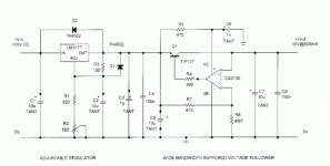
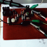
Based on a MAXIM design note http://www.maxim-ic.com/appnotes.cf...umber/169/ln/en I thought the design might have similar noise and ripple suppression characteristics to the Jung Super Reg. Although the design note described a low voltage application it should easily translate to a higher power version suitable for noise free on-board dc supplies for audio equipment. I built up a prototype (+12V) with a standard LM317T as a pre-regulator and supplied it from a transformer + bridge rectifier + 8000uF filter cap (~18V dc). The output of the LM317 reg was adjusted to supply 12.7V to the input of the voltage follower. A similar arrangement can be implemented for the negative supply using a LM337T and a NPN darlington.
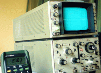
Loading the output to just over 800mA and connecting an oscilloscope at maximum sensitivity (5mV/div) I could not detect more than 1 or 2mV p - p ripple at most. A sensitive pair of headphones across the load revealed not one jot of noise of any kind. This design does not require huge reservoir capacitors onboard although when feeding high gain stages or sensitive equipment some additional capacitors would be beneficial.
It is noted that the voltage follower stage is not a regulator but is intended to provide around 40dB of additional ripple and noise rejection in the audio band up to 20KHz so it is intended to follow the output of this stage with an additional regulator.
Based on a MAXIM design note http://www.maxim-ic.com/appnotes.cf...umber/169/ln/en I thought the design might have similar noise and ripple suppression characteristics to the Jung Super Reg. Although the design note described a low voltage application it should easily translate to a higher power version suitable for noise free on-board dc supplies for audio equipment. I built up a prototype (+12V) with a standard LM317T as a pre-regulator and supplied it from a transformer + bridge rectifier + 8000uF filter cap (~18V dc). The output of the LM317 reg was adjusted to supply 12.7V to the input of the voltage follower. A similar arrangement can be implemented for the negative supply using a LM337T and a NPN darlington.
Loading the output to just over 800mA and connecting an oscilloscope at maximum sensitivity (5mV/div) I could not detect more than 1 or 2mV p - p ripple at most. A sensitive pair of headphones across the load revealed not one jot of noise of any kind. This design does not require huge reservoir capacitors onboard although when feeding high gain stages or sensitive equipment some additional capacitors would be beneficial.
It is noted that the voltage follower stage is not a regulator but is intended to provide around 40dB of additional ripple and noise rejection in the audio band up to 20KHz so it is intended to follow the output of this stage with an additional regulator.
Local Reg
MAXIM link didn't seem to work so here it is again
http://www.maxim-ic.com/appnotes.cfm/appnote_number/169/ln/en
MAXIM link didn't seem to work so here it is again
http://www.maxim-ic.com/appnotes.cfm/appnote_number/169/ln/en
- Status
- Not open for further replies.
- Home
- Amplifiers
- Solid State
- Local power regulators