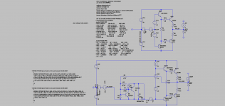
I recently performed an experimental validation of the use of a floating VBE multiplier to perform local linearization of an output stage. The idea is to regulate the voltage between the VAS and output to a constant value.
I researched this concept after an investigation of feedback versus "error correction" last year. OldDIY showed this strategy used in a Russian audio magazine. This implementation is an attempt to distill the benefits of Hawksford "error correction" documented by Jan Didden and LKA and others into a feedback concept with small parts count.
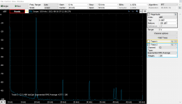
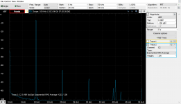
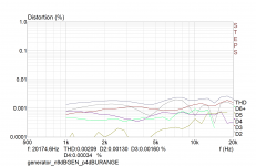
Attached is a schematic, generator baseline, output stage with feedback bypassed, and output stage with feedback. For the generator baseline, I set a scope to play a sine + DC offset into a DC coupled gain of 10 amplifier. This amplifier drove the output stage under test. The concept works nicely (tested with a bias of about ~20mA), resulting in about 10-15dB measured distortion reduction of the output stage with local feedback being reduced to the generator baseline. Results are shown for 5VPk or 10VPk-Pk into 8.2Ohms.
EDIT -> clarify difficult to read plots (better measurement is shown in post 4 with sound-card/global feedback)
Generator Harmonic 2 = -71dB
Generator Harmonic 3 = -72dB
Generator Harmonic 4 = -81dB
Output Stage (NO FB -> FB) Harmonic 2 = -59dB -> -71dB
Output Stage (NO FB -> FB) Harmonic 3 = -69dB -> -77dB
Output Stage (NO FB -> FB) Harmonic 4 = -70dB -> -80dB
EDIT
Some unexpected things came up with this development. I needed to set the Miller capacitor C1 higher than I thought to be stable. Initially I attempted a >1MHz bandwidth, but I settled on about a 400kHz bandwidth. I also needed to add R7 which helped the circuit find a good DC bias. The circuit feedback using R1 adds a bit more base current to drive this output stage from the VAS, but it is not terrible due to feedback making this fairly constant.
I added Q2 and R6 to increase linearization in simulation, and bypass C2 to control high frequency impedance. I also added zener diode D1 to clamp the output. I used high voltage transistors, but if I can establish the zener does not increase distortion, then lower voltage parts are potentially allowed. Unfortunately, I have reached the measurement limits of my current oscilloscope setup (Digilent Analog 2 + rat's nest) so I did not measure the distortion contributions of these circuit elements.
I did successfully incorporate this output stage into a broader amplifier circuit with 3rd order global feedback (this is the gain of 10 amplifier in front). The net result is stable. The whole amplifier circuit is easier to measure using a soundcard because it feeds back on the internal DC offset of the output stage. So I will do some modifications and measure with my RME UCX, but it may be hard to find the effects of Q2/R6/D1 in the presence of global feedback.
I researched this concept after an investigation of feedback versus "error correction" last year. OldDIY showed this strategy used in a Russian audio magazine. This implementation is an attempt to distill the benefits of Hawksford "error correction" documented by Jan Didden and LKA and others into a feedback concept with small parts count.
Attached is a schematic, generator baseline, output stage with feedback bypassed, and output stage with feedback. For the generator baseline, I set a scope to play a sine + DC offset into a DC coupled gain of 10 amplifier. This amplifier drove the output stage under test. The concept works nicely (tested with a bias of about ~20mA), resulting in about 10-15dB measured distortion reduction of the output stage with local feedback being reduced to the generator baseline. Results are shown for 5VPk or 10VPk-Pk into 8.2Ohms.
EDIT -> clarify difficult to read plots (better measurement is shown in post 4 with sound-card/global feedback)
Generator Harmonic 2 = -71dB
Generator Harmonic 3 = -72dB
Generator Harmonic 4 = -81dB
Output Stage (NO FB -> FB) Harmonic 2 = -59dB -> -71dB
Output Stage (NO FB -> FB) Harmonic 3 = -69dB -> -77dB
Output Stage (NO FB -> FB) Harmonic 4 = -70dB -> -80dB
EDIT
Some unexpected things came up with this development. I needed to set the Miller capacitor C1 higher than I thought to be stable. Initially I attempted a >1MHz bandwidth, but I settled on about a 400kHz bandwidth. I also needed to add R7 which helped the circuit find a good DC bias. The circuit feedback using R1 adds a bit more base current to drive this output stage from the VAS, but it is not terrible due to feedback making this fairly constant.
I added Q2 and R6 to increase linearization in simulation, and bypass C2 to control high frequency impedance. I also added zener diode D1 to clamp the output. I used high voltage transistors, but if I can establish the zener does not increase distortion, then lower voltage parts are potentially allowed. Unfortunately, I have reached the measurement limits of my current oscilloscope setup (Digilent Analog 2 + rat's nest) so I did not measure the distortion contributions of these circuit elements.
I did successfully incorporate this output stage into a broader amplifier circuit with 3rd order global feedback (this is the gain of 10 amplifier in front). The net result is stable. The whole amplifier circuit is easier to measure using a soundcard because it feeds back on the internal DC offset of the output stage. So I will do some modifications and measure with my RME UCX, but it may be hard to find the effects of Q2/R6/D1 in the presence of global feedback.
Attachments

Last edited:
Some unexpected things came up with this development. I needed to set the Miller capacitor C1 higher than I thought to be stable. Initially I attempted a >1MHz bandwidth, but I settled on about a 400kHz bandwidth. I also needed to add R7 which helped the circuit find a good DC bias. The circuit feedback using R1 adds a bit more base current to drive this output stage from the VAS, but it is not terrible due to feedback making this fairly constant.
If you use the same output stage with CFA input stage and VAS, I believe you can get >1MHz easily.
Considering few number of components here, I expect you can get >5MHz bandwidth out of it. You could only settle to 400KHz, I believe something must be missing here.
With that bandwidth >5MHz, the whole thing can be used as an single output stage with gain. Then, we can wrap another Global feedback to further lower the distortion.
Edit: I reviewed the schematic more carefully. It may not feasible to have gain. It works as unit gain. It is still pretty cool though if you can make it work.
Last edited:
Thanks for the vote of confidence on the bandwidth. I changed the local miller capacitor to 100pF || 100kOhm, and obtained stable operation with about 1MHz bandwidth and 37dB total local loop gain.
While yesterday's measurements focused on the local loop, this is indeed intended for unity gain output stage linearization in the presence of a global feedback network. I did some analysis and found my global loop limiting yesterday and now I've been able to further push the local loop. I am currently at 34dB local gain + 55dB global = 89dB total loop gain at 20kHz.
While yesterday's measurements focused on the local loop, this is indeed intended for unity gain output stage linearization in the presence of a global feedback network. I did some analysis and found my global loop limiting yesterday and now I've been able to further push the local loop. I am currently at 34dB local gain + 55dB global = 89dB total loop gain at 20kHz.
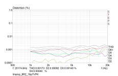
Here is the distortion performance measured using my sound card (RME UCX) to measure the complete amplifier with global feedback. Level is 11.8VRMS into 8.2Ohms which was selected to respect the voltage and current protection limits on the prototype. Measurement sample rate is 192kHz (or 96kHz Nyquist).
The first picture is the sound card loop-back at those levels. The second is the measured amplifier performance, which is indistinguishable from the sound card loop-back. I believe the minor differences in levels (the plots are not mixed up) relate to the gain/attenuator used on the test article.
The first picture is the sound card loop-back at those levels. The second is the measured amplifier performance, which is indistinguishable from the sound card loop-back. I believe the minor differences in levels (the plots are not mixed up) relate to the gain/attenuator used on the test article.
Attachments
Here is what I came up with.
Near 60dB local feedback. Output stage is biased at 100mA. Generally, the more bias, the more bandwidth.
The unit loop gain frequency is around 4MHz. Serial a zero-nulling resistor with Miller cap is kind of required to get extra bandwidth of it.
I also simulated square wave, you can see there is overshot, but there is no ringing (almost). If you put it behind a normal VAS (limited bandwidth), there should be no overshot.


BTW, that's 100KHz square wave.
Near 60dB local feedback. Output stage is biased at 100mA. Generally, the more bias, the more bandwidth.
The unit loop gain frequency is around 4MHz. Serial a zero-nulling resistor with Miller cap is kind of required to get extra bandwidth of it.
I also simulated square wave, you can see there is overshot, but there is no ringing (almost). If you put it behind a normal VAS (limited bandwidth), there should be no overshot.
BTW, that's 100KHz square wave.
Last edited:
I figured out that if you only involve 2 components in the feedback, you don't need Miller cap, and it is unconditional stable.
Here is my latest implementation. NFB with Vbe Multiplier, Better Than CFP?
Here is my latest implementation. NFB with Vbe Multiplier, Better Than CFP?
Thank you for your comments. I also considered a series R+C in parallel with my schematic's R1 to introduce lead. I am pretty happy with the performance of the 1MHz version right now, but I need to double check its frequency response for peaking. I am a little nervous about going too much higher due to questions about the SPICE models and test probes at high frequencies.
I think the version I prototyped is sufficient for now (with global feedback) because I would need to invest in an improved test jig to measure better than 0.002% at 20kHz (which is state of the art for power electronics already). The version you linked looks clever for achieving linearization at very high frequencies. One comment I have to your pictures in this thread and the other one is that I chose a higher bias voltage than you did because it linearizes the local feedback amplifier's transistors a little better.
I asked a question in your thread about the implications of your version on the thermal bias. I put the VBE multiplier outside the bias circuit so that it would not impact it. I did explore differential versions, which have the nice characteristic of avoiding windup without requiring a zener.
Last edited:
Thanks for bringing the research in the other thread to my attention OldDIY. The differential Rush VBE multiplier they use appears inside out relative to mine. I will have to think about what effects this has. I wonder why they went as far as to linearize each half, but stopped short of taking feedback on the whole.
I did another simulation recently to determine how much feedback is enough (ie what linearization bandwidth should one try for). Attached is a quick LTSpice simulation which takes the base current from the emitter follower with and without linearization and injects it into a basic VAS stage. With the double EF, I found that after about 20dB of local linearization, the base currents injected into the VAS start to dominate the total distortion. The cure I used in this simulation was to buffer the VAS to lower its output impedance (which can be turned on or off by shorting the resistor in parallel with the EF buffer).
I did another simulation recently to determine how much feedback is enough (ie what linearization bandwidth should one try for). Attached is a quick LTSpice simulation which takes the base current from the emitter follower with and without linearization and injects it into a basic VAS stage. With the double EF, I found that after about 20dB of local linearization, the base currents injected into the VAS start to dominate the total distortion. The cure I used in this simulation was to buffer the VAS to lower its output impedance (which can be turned on or off by shorting the resistor in parallel with the EF buffer).
Attachments
Thanks for the link OldDIY. The folded cascode arrangement is quite attractive for use with an opamp front end due to its limited voltage input range. The feedback nodes are similar to the floating concept I used, but the folded cascode version should be reduced capacitance distortion due to the higher working voltages.
I've had some good laboratory progress with my circuit, but also some struggles. I've been using the version with 1MHz feedback bandwidth for a few weeks. It exhibits good startup and shutdown behavior, graceful clipping and current limiting, and does not have any out of band resonances. I have struggled with measuring the circuit with global feedback because minor changes in my ground return path can change results from -80dB to -100dB THD. I will be making some investments in a ground cancelling line driver and improved power supply wiring so I can accurately quantify system performance.
I've tried to determine whether there are any improvements I can make to the local feedback circuit in simulation space. For currently related distortions, I can change the Q2 collector to connect to the rail to avoid passing base currents to the VAS. For voltage distortions, there are some options to pick lower capacitance transistors, but the simulations indicate it has to get worse by about a factor of ten from the models to make a difference.
- Home
- Amplifiers
- Solid State
- local output feedback using floating VBE multiplier