Dear all,
I just build an effects loop with a couple of LND150's. Not all was going as smooth as normal. I was stupid enough to draw the mosfets backwards in Eagle and place them accordingly (D and S swapped). Turned them around and the recovery stage seems to work fine now (direct guitar in the return path gave a non distorted output).
The problem is with the send side of the loop. A strange 1.4 V p-p slow sinus (or oscillation?; around 10 Hz) is continuously present after the follower. The sound cuts in and out at the same speed.
What could this be? Faulty mosfet, limiter leds, a not working type of bootstrapping or something else?
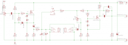
Schematics are attached. Everything sims fine with ltspice though. The loop I build is the fourth from the top in the ltspice file. I know simulation =/ reality...
I just build an effects loop with a couple of LND150's. Not all was going as smooth as normal. I was stupid enough to draw the mosfets backwards in Eagle and place them accordingly (D and S swapped). Turned them around and the recovery stage seems to work fine now (direct guitar in the return path gave a non distorted output).
The problem is with the send side of the loop. A strange 1.4 V p-p slow sinus (or oscillation?; around 10 Hz) is continuously present after the follower. The sound cuts in and out at the same speed.
What could this be? Faulty mosfet, limiter leds, a not working type of bootstrapping or something else?
Schematics are attached. Everything sims fine with ltspice though. The loop I build is the fourth from the top in the ltspice file. I know simulation =/ reality...
Attachments
Hi Guys
The negative end of C5 should be grounded.
Lose the LEDs.
Lose the downward-facing zeners in the gate protection.
What is the supply voltage? It is likely much better to adjust the voltage divider (R2,3) to be 470k on top and 100k on bottom if you are using 300V input.
The return amp is a bit mixed up, too. The gate should have a resistive path to ground that is capacitively coupled to the feedback network. The return pot should have a resistor in series with it otherwise the mixing function will be defeated with the pot dialled to zero-ohms. Obviously an attempt to have variable return gain, which is do-able this way but not ideal.
The input divider and pot will reduce the entire loop signal and not be a Send control per se, if the latter was the intent.
The LND150s have been around for quite a while and are universally used incorrectly in these loop apps. They do not work well at the voltages inside a guitar amp and need a clamped or regulated supply.
The Effects Loops chapter of TUT shows a much better high-voltage solid-state loop.
Have fun
Last edited:
C5 was indeed the culprit. Bootstrapping this way doesn't work here it seems and introduces a very low frequency oscillation. Ditched it and all is fine now. There wasn't room enough on the pcb to put the cap over the lower bias resistor (R2).
Now your answers and suggestions lead to more questions Struth. I always want to know why, maybe that's just me. I know about those books (your writings I guess). They seem to be a good source of ideas and knowledge.
Adjusting the voltage divider network R2/3 gave me higher distortion when I lowered the lower resistor. That was in ltspice however. Could you elaborate why that would be different in real life?
The send pot is before the follower to keep the output impedance fixed. Should be around 600 Ohms this way. The send control is essentially a master volume before the loop and is only effective when the loop is on.
The return path/level control is done by varying the amount of nfb around the recovery stage. Although the sweep of the return pot is a bit awkward, it works as intended. Not ideal I admit. Distortion rapidly rises when the return level is set higher and input impedance drops to a meagre 22k or so.
R5 sets the minimal value for the nfb. That's 4meg7/22k divider, which is almost no nfb.
Q2 gate sees a path to ground through R5/8/9/10, right? Am I missing something?
R7 needs to be adjusted to get a proper mixing level and a usable sweep. It isn't satisfactory now: big volume jump towards the wet side with line level effects signal.
B+ is around 300V and taken from the PI. Parallel to the PI that is. I adjusted the dropping resistors before the PI.
You say LND150's aren't working well with the voltages inside a guitar amp. Why not? Are they really only good at switching at higher voltage? Is there an alternative? BS170, DN2540 or something along those lines?
Could you point me to a better design that is not only available in hard copy? I'd like to learn by building, reviewing and as you already stated 'having fun'.
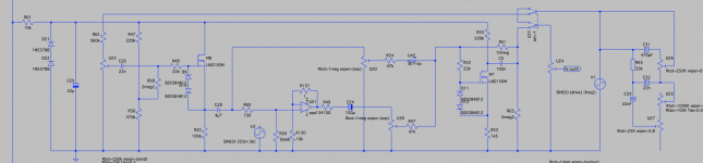
The loop worked almost first time. Swapped D and S in Eagle so I placed the mosfets the wrong way around. My bad. Good thing is the Mosfets survived (due to the zeners?).
Take a look at the available space for the loop. Not much room to expand left...
Now your answers and suggestions lead to more questions Struth. I always want to know why, maybe that's just me. I know about those books (your writings I guess). They seem to be a good source of ideas and knowledge.
Adjusting the voltage divider network R2/3 gave me higher distortion when I lowered the lower resistor. That was in ltspice however. Could you elaborate why that would be different in real life?
The send pot is before the follower to keep the output impedance fixed. Should be around 600 Ohms this way. The send control is essentially a master volume before the loop and is only effective when the loop is on.
The return path/level control is done by varying the amount of nfb around the recovery stage. Although the sweep of the return pot is a bit awkward, it works as intended. Not ideal I admit. Distortion rapidly rises when the return level is set higher and input impedance drops to a meagre 22k or so.
R5 sets the minimal value for the nfb. That's 4meg7/22k divider, which is almost no nfb.
Q2 gate sees a path to ground through R5/8/9/10, right? Am I missing something?
R7 needs to be adjusted to get a proper mixing level and a usable sweep. It isn't satisfactory now: big volume jump towards the wet side with line level effects signal.
B+ is around 300V and taken from the PI. Parallel to the PI that is. I adjusted the dropping resistors before the PI.
You say LND150's aren't working well with the voltages inside a guitar amp. Why not? Are they really only good at switching at higher voltage? Is there an alternative? BS170, DN2540 or something along those lines?
Could you point me to a better design that is not only available in hard copy? I'd like to learn by building, reviewing and as you already stated 'having fun'.
The loop worked almost first time. Swapped D and S in Eagle so I placed the mosfets the wrong way around. My bad. Good thing is the Mosfets survived (due to the zeners?).
Take a look at the available space for the loop. Not much room to expand left...
Hi Guys
Those little LND mosfets came out back in the early 2000s and lots of amp builders were interested in them. They seem ideal looking at the spec sheet inasmuch as you can drop it into a Fender-value stage and it works. The claimed voltage rating also seems adequate but it isn't truly for most amps.
However, their dissipation rating is very limiting as is their current rating.
There are many details about designing effects loops that I am not going to state here - that is why i wrote the book on it - but suffice to say, there is no reason to bypass a loop circuit completely when it is not in use. Those who think you must do not know how to design a proper loop. The fact you are using LTspice puts you a few steps ahead of that crowd... haha... but...
The loop is usually placed at a line-level circuit point. What is line level? Think of it as whatever is needed to drive the power amp to clipping, so maybe 2V peak at most for standard PA designs. This means the signal in the loop is only ever this amplitude. The only problem you run into is if you want to use pedals then the signal being sent must be attenuated and the returning signal must be boosted by the reciprocal amount. When you have a single gain element like the LND it will distort if you ask for too much gain and the feedback loop will not work quite as it should. Tubes do the same thing. The "however" here is that the signals are small so the distortion is not very high.
LNDs used in commercially available loop kits tend to die in real amps. This is because the designers of such things skimp on essentials, in this case, there is no supply clamp. A few zeners in series will protect the devices and provide a performance improvement as well. The small size of the LNDs possibly contributes to the zeal to create a super-small loop footprint and this requires leaving out stuff that should not be left out. "Things should be as simple as required but no simpler".
In your circuit, there is no reason for the send coupling cap to be 450V. Reverse the divider values or adjust them as I suggested and you can use a 100V part there. Same for the filter across the divider, which does not have to be 47uF, rather 10uF max. Adding this cap greatly improves the hum and noise figure.
Yes, your return mosfet gate has a DC path to ground but doing it that way tends to introduce a gain error in the loop. I always AC couple there and it is a bit more accurate. The gain inaccuracy is common to all technologies and is is easily seen by a few simple calculations of open-loop to closed-loop ratios: the greater the open-loop gain the more predictable the closed-loop gain will be.
An intuitive alternative to the LND is simply to use TO-220 mosfets. These are available up to 1kV and at ample power ratings to run in free air. However, their gate capacitance will be problematic and a cascode or alternate circuit improves things immensely. You can also simply reduce the voltages to 50V say and have much more lattitude with biasing.
Have fun
A very long time ago I read an electronics book which pointed out that this type of bootstrapping introduces a big hump in the frequency response, usually well below 20 Hz. The hump is caused by the combination of positive feedback, along with phase shift from the capacitors in the circuit. The size of the hump depends on specific component values used.C5 was indeed the culprit. Bootstrapping this way doesn't work here it seems and introduces a very low frequency oscillation.
I can no longer remember the author of the book. But this was long before LTSpice or personal computers capable of running it existed. The author discovered the problem by mathematical analysis of the transfer function of such a circuit.
The usual problem caused by the "hump" is a type of blocking distortion - a transient with sufficient low-frequency energy can trigger the circuit to block, sometimes for seconds at a time.
This was particularly likely to be a problem when this type of bootstrapping was used with a turntable with a piezo cartridge. Piezos require high input impedance, so bootstrapping seemed the logical solution - but cheap turntables with piezo cartridges were also prone to produce enough rumble to trigger the circuit into blocking.
As you found out, the it is even possible to get sustained low frequency oscillation from this circuit, in extreme circumstances.
Luckily, you don't need bootstrapping in this application. There's no need for super-ultra-high input impedence on the send side. R_in is already over 2.2 megaohms without bootstrapping!
Also, I don't think 470 ohm gate-stopper resistors are enough to keep fast little MOSFETs like this from oscillating. I would increase those quite a bit, to 22k or so.
Anyway, I'm glad all is well now!
-Gnobuddy
Thanks for your lengthy answere (a good thing!). Pretty late here, so I'm going to keep it short. What do you mean by clamping? Regulating with a series resistor and a zener to ground or zeners in series between the pi node and the loop? What is the purpose? Limit voltage spikes? Thanks again.
Thanks for the reply Gnobuddy. I should have know, simulation revealed a 30dB bump well below 20 Hz indeed. At first I only looked between 20 Hz and 20 kHz, already more than what is of interest for guitar.
I'll change those gay-stoppers. Increasing them will not harm anything AFAIK.
I'll change those gay-stoppers. Increasing them will not harm anything AFAIK.
You're quite welcome!
30 dB is an impressive peak. I just spent a little time with LTSpice trying to create a peak in a similar circuit, but the worst I managed was only about 11 dB. 🙂
It's been a long time since I read that book, but IIRC the ratio of C5/C1 is one of the things that sets the height of the peak. Your circuit happens to have a very large ratio of C5/C1, around 2000:1. That's probably part of the reason for such a huge (30 dB) peak.
I suspect that additional phase shifts from other components (perhaps from power supply decoupling capacitors) are required to get actual oscillation. Another reason why the problems tend to surface well below 20 Hz, when the decoupling capacitors can no longer be treated like AC short-circuits.
Now you have me wondering if we can get something useful out of this circuit, by deliberately using that peak. A combined bass-cut and midrange boost might be useful, in some cases, like a wah-wah pedal set to one position!
-Gnobuddy
With the bootstrap cap I was asking for problems like LFO. It seems that the higher the ratio between C1/C5, the less the effect. As there is no clear advantage to be had here, I dropped the idea.
Now would a self biasing arrangement work, like seen in many tube LTP's or tube Cf's in effects loops? Simulation predicts it would work, but I rarely see any schematics employing a self biased source follower. Why is that? Also a concept prone to design flaws?
Anyway, I agree with Kevin (if you allow me to be on a first name basis) that the return stage was a bit of a mixed bag. So I borrowed an idea from Engl and that is to put a stereo pot before the return stage. When one pot goes up, the other goes down. This makes the results much more predictable than before, with the last stage becoming more of a switchable mixer (as you can switch out the parallel side).
Due to design limitations, THD is rather high (but it's in a guitar amp anyway).
In parallel mode the value of the stereo pot largely influences the the available gain of the return stage. Lower values give better gain when the pot is set around half, but the taper tends to be more linear then.
I thought, I put up my thoughts again. In the end they might help someone and I just like to experiment anyway, so what's not to love 😀
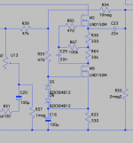
Ps. I added a zener clamp. I suppose that is what you meant Kevin?
Now would a self biasing arrangement work, like seen in many tube LTP's or tube Cf's in effects loops? Simulation predicts it would work, but I rarely see any schematics employing a self biased source follower. Why is that? Also a concept prone to design flaws?
Anyway, I agree with Kevin (if you allow me to be on a first name basis) that the return stage was a bit of a mixed bag. So I borrowed an idea from Engl and that is to put a stereo pot before the return stage. When one pot goes up, the other goes down. This makes the results much more predictable than before, with the last stage becoming more of a switchable mixer (as you can switch out the parallel side).
Due to design limitations, THD is rather high (but it's in a guitar amp anyway).
In parallel mode the value of the stereo pot largely influences the the available gain of the return stage. Lower values give better gain when the pot is set around half, but the taper tends to be more linear then.
I thought, I put up my thoughts again. In the end they might help someone and I just like to experiment anyway, so what's not to love 😀
Ps. I added a zener clamp. I suppose that is what you meant Kevin?
Attachments
Hi Guys
The supply clamp is good!
I still don't see why you have the buffer biased to 2/3 of the supply? Where in the signal path is this loop and how much signal do you expect? R56 really should have a cap across it. With the values of the divider, a value less than 1uF will provide flat response.
Is the opamp supposed to represent an effect in the loop?
In most loops with variable gain, a linear dual-pot is used and the send signal is reduced while the return gain rises and vice-versa. Most of these loops are series-only and the pot is just to accommodate pedals or line-level. The same approach can be used in mix mode with no pot on the dry path.
The bootsrtapping to increase input impedance is not needed with divider bias, as you have. With the cap added across R56, there is no noise penalty using a high value gate-leak. In a self-bias follower, bootstrapping of the gate-leak is inherent.
Have fun
That clamp is there on your advise, so thanks! Should be a good protection against voltage spikes. The rest of the amp is very old school, so there is no other protection against spikes.
The divider is still that high (2/3) because lowering the values leads to an increase in distortion - mainly second order - of the follower. This gives the lowest values possible. I suppose you have taken real life measurements with a scope. I didn't and thus have relied on sims (and not on your advise, yet!). Does a bias around 40 or 50V indeed increase second harmonics in real life, and if so, how bad is het effect? I also see the advantage of a lower voltage cap after the follower, although the 450V was already pretty cheap (€ 0.60 IIRC).
The op amp is an effect. This way I can alter the gain of the effect by just changing the feedback resistor. Sometimes I replace the op amp with a voltage source set to a different frequency (e.g. 3k Hz) than the main test signal (1k Hz), so I can simulate the working of the mixing in parallel mode.
Marshall uses a system with a switch that toggles between -20dB and 0dB in a manner you describe. Lowers the send signal and at the same time increases the return gain. Pretty clever and common, but it gives very little control over the signals in the loop. Time will tell if I need all those options. Probably not, but designing and building this way is a big part of the fun .
.
Will add a 1uF cap to R56!
Bootstrapping of the gate-leakage means higher power consumption, right? Or also higher noise?
Anyhow, the concept of a loop in an old school amp is flawed anyway. Whit PI and power tube saturation the effect will distort. Been working on a attenuator with a loop lately. Even with simple devices like TL072's it is a piece of cake to get better results THD wise than with two LND150's. Now if I'd go for some more exotic stuff with LND150's, that'd be different...
The divider is still that high (2/3) because lowering the values leads to an increase in distortion - mainly second order - of the follower. This gives the lowest values possible. I suppose you have taken real life measurements with a scope. I didn't and thus have relied on sims (and not on your advise, yet!). Does a bias around 40 or 50V indeed increase second harmonics in real life, and if so, how bad is het effect? I also see the advantage of a lower voltage cap after the follower, although the 450V was already pretty cheap (€ 0.60 IIRC).
The op amp is an effect. This way I can alter the gain of the effect by just changing the feedback resistor. Sometimes I replace the op amp with a voltage source set to a different frequency (e.g. 3k Hz) than the main test signal (1k Hz), so I can simulate the working of the mixing in parallel mode.
Marshall uses a system with a switch that toggles between -20dB and 0dB in a manner you describe. Lowers the send signal and at the same time increases the return gain. Pretty clever and common, but it gives very little control over the signals in the loop. Time will tell if I need all those options. Probably not, but designing and building this way is a big part of the fun
.Will add a 1uF cap to R56!
Bootstrapping of the gate-leakage means higher power consumption, right? Or also higher noise?
Anyhow, the concept of a loop in an old school amp is flawed anyway. Whit PI and power tube saturation the effect will distort. Been working on a attenuator with a loop lately. Even with simple devices like TL072's it is a piece of cake to get better results THD wise than with two LND150's. Now if I'd go for some more exotic stuff with LND150's, that'd be different...
Hi Guys
Rootz, you need to look at more schematics and more books. Marshall had continuously variable loop gain as i described.
"Anyhow, the concept of a loop in an old school amp is flawed anyway. Whit PI and power tube saturation the effect will distort."
How does the effect distort unless you place it after the PA? Your statement more correctly implies that the output sound of the effect will be distorted when the output stage clips, but so would that effect output be distorted were it plugged through the input of the amp. Clipping trumps everything.
Whether a non-MV amp should have a loop or not is purely aesthetic and every opinion is correct.
The clamp is not there to protect against spikes, rather to keep the voltage to the LNDs within their ratings during all conditions of the amp's supply. Increased THD is not a worry until it becomes audible. The return amp feedback resistor does not look like it provides much in the way of actual feedback - a flaw of using a single device and one of all the LND circuits implemented so far.
Have fun
I could use more books! Other that yours and Merlin's there doesn't seem to be many books on the topic of loops alone (or a good chapter about it), let alone MOSFET loops. At least not to my knowledge. Guess part of my next pay check goes to other side of the pond (your side, that is...).
Schematics tell what is done, not why. I takes me (a lot) of time to figure out some of the design considerations when just looking at schematics. Not terribly efficient, but it's fun to have those Eureka moments and understand what is done and why!
I should have been more precise when I mentioned a Marshall effects loop. They are clearly not all the same. I was referring to the op amp loop used in the 1959 and 2203 reissue amps.
You are correct I was implying on distortion of the PA that trumps the effect you put in a loop that is before the PA. That's why I'm working on a loop after a reactive attenuator, which essentially turns my non-MV amps into a 40lb. distortion boxes. Great sounding distortion boxes 🙂. No way I'm going to drill more holes in my JTM45! That is largely because I suspect that an effect in a loop before the PA will only sound marginally better than that same effect in front of the amp, especially in a non-MV amp. The loop I built is in a MV amp (Marshall 2204 variation), that I turn up to the point of clipping through a attenuator. I'm yet to find out how it behaves with a delay in the loop; wether it's useless or not.
The feedback is indeed minimal when the loop return is turned up. There is only much feedback at lower return settings. Thus THD rises when you turn up the return. Influencing the feedback with the return pot is the biggest part of this loops concept. What should I say? It works, but could be better.
Now I've been working on multi device send and return stages. For example a mu-follower as a return with the same concept of variable feedback gives much better results THD wise at a much higher output voltage. It seems to me that you'd need to pay close attention to matching the top and bottom Fets and resistors in such arrangements, am I right?
Attachments
Last edited:
Yes, very much so! As flawed as Donald Trump! 😀Now would a self biasing arrangement work, like seen in many tube LTP's or tube Cf's in effects loops? Simulation predicts it would work, but I rarely see any schematics employing a self biased source follower. Why is that? Also a concept prone to design flaws?
The problem is that FETs have very wide parameter spreads (very poor manufacturing tolerance) where it's really critical for the values of Idss and Vp. They often vary over a 3:1 range, which is horrible - loosely speaking, 300% variation!
What this means in practice is that if you pull five supposedly identical FETs out of a bag and plug them into the same self-biased circuit, some will work, some will be deep in saturation, some will be almost cut-off, and probably not one of them will work exactly the way you intended it to work!
Bipolar junction transistors have wide spreads in current gain, but at least they have a predictable base-emitter voltage, and the collector voltage doesn't affect the collector current much. So you can design a circuit with confidence that it will work with, say, any BC147 transistor.
Valves have surprisingly good tolerances - often within a few percent of each other. So once again, we can design a simple self-biased 12AX7 stage, and it will work with every 12AX7 you plug in.
There is no such guarantee with FETs, whether JFET or MOSFET. Usually the tolerances are so bad that you have to design the circuit to be able to absorb the normal fluctuations in Vgs from one FET to the next one.
One very good way to do this is to use a large source resistor, and apply many volts between the gate and the far end of that resistor. If we have, say, 20 volts DC across the resistor, it doesn't matter if Vgs changes by +/- 2 volts due to FET tolerances; that will only be a change from 18V - 22V, which is about +/- 10% in the source current. No problem.
If you try to self-bias the same JFETs, and expected Vgs is 3 volts, you now have a spread of 3V +/- 2V. That means a possible variation from 1V to 5V: up to 500% variation in source current! Obviously, an impractical solution.
Sorry about the delayed reply, I have been a bit busy!
-Gnobuddy
There may be a fringe benefit to the high bias voltage: it reduces the total voltage across the FET (Vds). That means less total power dissipation in the FET. This is a good thing in a tiny TO92 FET like the LND-150.The divider is still that high (2/3) because lowering the values leads to an increase in distortion - mainly second order - of the follower. This gives the lowest values possible.
The distortion reduction you simulated is probably real, at least on paper: higher bias voltage on the gate means a larger value of the external source resistor Rs. That means the ratio of the nonlinear *internal* source resistance (rs, equal to 1/gm of the FET) to the external, linear one (Rs) falls; and a lower ratio (rs/Rs) in turn should lower distortion.
It may be real, but is this distortion significant? In a guitar amp, my opinion is that it doesn't matter at all. A guitarist will dial up what she calls a "clean tone", that might in fact contain 10% or more harmonic distortion. If the FET source follower is contributing 0.1% distortion at the same time, it is completely insignificant, orders of magnitude below the total harmonic distortion, therefore completely inaudible.
Surprisingly large amounts of second harmonic distortion, by the way, seem to still be a good thing in a guitar amp, in the sense that it sounds good.
-Gnobuddy
- Status
- Not open for further replies.
- Home
- Live Sound
- Instruments and Amps
- LND150 effects loop not working properly, need help.