now we find the datasheet for the LME49830 on
www.national.com
The Eval-board use IRFP240/9240
It is a good idea to give the LME a own power supply,
maybe ±50V, and use ±40V for the HexFets-powerstage?
www.national.com
The Eval-board use IRFP240/9240
It is a good idea to give the LME a own power supply,
maybe ±50V, and use ±40V for the HexFets-powerstage?
You will get more output power from the FETs this way but it might not be worth the effort depending on what you actually want to accomplish. You might just want to increase the supply voltage to get what you want. The advantage is more output power from the FETs and higher peak efficiency since there is less wasted voltage.
-SL
-SL
Thanks
I must explain, what I like to do.
I will use one Transformer and make a voltage-double
with stabilisation for the LME49830.
If I like to have a very good amplifier, it's maybe the
best way to use a stabilized supply, but it must be enough
to do this for the voltage-amplifier (LME49830).
sample circuit
Take a lookat this if you haven't already seen it:
http://www.passdiy.com/pdf/A75p1.pdf
and especially this:
http://www.passdiy.com/pdf/A75p2.pdf
http://www.passdiy.com/pdf/A75p1.pdf
and especially this:
http://www.passdiy.com/pdf/A75p2.pdf
especially the Pass_A75p2.pdf is a must read,
thank you very much
Next questions,
on the National-Eval-Board the RQ ist located near by
the hexfets.
RQ is a resistor-load for the LME, not a termination,
so I like to place it near the LME.
I'm wrong?
thank you very much
Next questions,
on the National-Eval-Board the RQ ist located near by
the hexfets.
RQ is a resistor-load for the LME, not a termination,
so I like to place it near the LME.
I'm wrong?
Power supply
If you're going to the trouble of powering your output devices differently from the driver chip, I'd suggest a higher voltage on the MOSFETs, which have a substantially greater voltage drop between supply and max output than bipolars. Why would you want to send less voltage to the outputs? Take a look at the Hafler designs.
If you're going to the trouble of powering your output devices differently from the driver chip, I'd suggest a higher voltage on the MOSFETs, which have a substantially greater voltage drop between supply and max output than bipolars. Why would you want to send less voltage to the outputs? Take a look at the Hafler designs.
Originally posted by craigg4c
If you're going to the trouble of powering your output devices differently from the driver chip, I'd suggest a higher voltage on the MOSFETs, which have a substantially greater voltage drop between supply and max output than bipolars. Why would you want to send less voltage to the outputs? Take a look at the Hafler designs.
Mosfets need to have the gate driven over theyr drain to fully conduct, so if they are powered from higher rails than the driver stage you will always be wasting power there.
The main advantage of powering the driver stage with a different supply is that it can have a much cleaner power and this improves the result.
most FET amplifiers perform better if the output bias is set high.
This dissipates a lot of heat.
Using the highest acceptable FET supply voltage to meet your target power, and output voltage requirements gets best efficiency and best economy from your PSU and heatsink and FETs.
Using a slightly higher and clean voltage PSU for the voltage amp stage is perfectly acceptable and does not add much in the way of volume nor cost to the project but does allow improved performance from the overall package.
Extra LV windings on the mains toroid is the cheap and easy way to get your increased voltage. Voltage doublers have their own problems, particularly if the driver stage consumes high continuous or transient current.
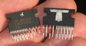
I'm quite surprised that national is selling a FET driver, my experience with the LME49810 shows that it's perfectly capable of driving HEXFETS and it sounds very, very good with them. I prefer the IRFP's over the toshiba's more expensive pair (2SK1530 & 2SJ201).
Kay (or anyone else), Have you tried to build an amp with the LME49830 and one with the LME49810 and noticed any difference?
Kay (or anyone else), Have you tried to build an amp with the LME49830 and one with the LME49810 and noticed any difference?
The differences between the LME49810 and LME49830 is the 810 has the baker clamp and clip indicator pin. If you look at the two datasheets and the diagrams then you will see some slight differences. Then the 810 has lower maximum bias voltage. May not matter for most FET uses. But you can use any of the National drivers for either BJT or FET output stages.
-SL
-SL

Dxvideo said:A question;
The pin "OSENSE" of LME49830 is for a kind of current limiting for output devices?
Hi Dxvideo.
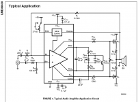
From the datasheet we can read following.
I attach Figure 1 = typical amplifier application.
OUTPUT SENSING
The Output Sense pin Osense must be connected to the system output as shown in Figure 1.
This connection completes the return path to feedback the output voltage to the mute gain circuitry inside LME49830.
If the Osense pin is not connected to the output or it is floated,
high voltage generated from the output stage may cause damage to the speaker or load.
Attachments
lme 49830
I am trying to use it as a 20 watt test amp for speaker analisys and was wondering if there are anything to be aware if running it with out transistor in the output stage
I am trying to use it as a 20 watt test amp for speaker analisys and was wondering if there are anything to be aware if running it with out transistor in the output stage
Bias circuit for Laterals
Hi,
😕
I am trying to adjust the bias circuit of the LME49830 but I can not make it work properly. Has someone tried it with Lateral mosfet where the bias voltage between N and P channels needs to vary from about 1 to 3 Vdc. Because of lower gate voltage of lateral I changed the 1.2K resistor in seris with VBE multiplier by 100 ohms....is it correct? 🙄
Thanks
Fab
- Status
- Not open for further replies.
- Home
- Amplifiers
- Chip Amps
- LME49830 with (HEX)Fets