Hi everyone!
Because LM3886 is nowhere to find (out of stock), it will be nice to have a discrete substitute design!
I have created simulation of an amp in LTSpice simulator. I have tried to stay as close as possible to the internal LM3886 schematics.
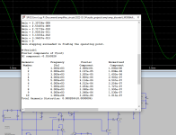
THD is 0.0002% for 2V input at 1kHz.
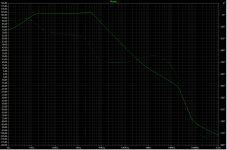
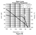
OLG is >70dB at 20kHz.
Attached are schematics and files.
I am also planning on making SMD / THT board that will have similar outputs as LM3886, namely inverted input, non-inverted input, etc..
As far as protections, I am planning on using four diodes: from each rail to ground, and from each rail to output of an amp.
Any other suggestions for the protection will be helpful.
Not sure about phase margin stuff yet....
Let me know if I missed anything, appreciate any input.
Because LM3886 is nowhere to find (out of stock), it will be nice to have a discrete substitute design!
I have created simulation of an amp in LTSpice simulator. I have tried to stay as close as possible to the internal LM3886 schematics.
THD is 0.0002% for 2V input at 1kHz.
OLG is >70dB at 20kHz.
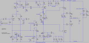
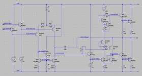
- Mainly for the input stage we have long tail pair arrangement loaded with current mirror that employs a helper transistor. Constant current source is supplying 2mA and created with two transistors.
- For voltage amplification section LM3886 is using two transistor emitter follower configuration. There is some kind of buffering happening, but I lack expertise to determine what it is. Instead it was replaced with Hawksford enhanced cascode.
- Miller compensation was replaced with two pole compensation. On the board I plan to have ability to switch between two. Also, thinking about adding option to do transitional Miller compensation. So in total three different compensations to select using jumpers on the board.
- For output stage it is a simple 2EF (two transistors emitter follower) with driver and output transistors.
Attached are schematics and files.
I am also planning on making SMD / THT board that will have similar outputs as LM3886, namely inverted input, non-inverted input, etc..
As far as protections, I am planning on using four diodes: from each rail to ground, and from each rail to output of an amp.
Any other suggestions for the protection will be helpful.
Not sure about phase margin stuff yet....
Let me know if I missed anything, appreciate any input.
Attachments
Last edited:
Is there any DC bias on C3?
Some tests you could try: put a resistor across the input, use a signal generator with a DC offset for the power rails and find out what happens at the audio output.
Some tests you could try: put a resistor across the input, use a signal generator with a DC offset for the power rails and find out what happens at the audio output.
Last edited:
I don't know, you are talking about a LM3886 substitute, but the schematic you presented is a completely different amplifier. Different input stage, output stage, compensation, passives values. Three times faster than the LM3886, twice the loopgain at 10kHz. Not judging your design by any means, but I would not call it a LM3886 substitute.
If you are after a LM3886 substitute:
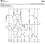
I have a simulation model, which I created to double check the spice models given by TI with a discrete design. The circuit is virtually identical to the internal LM3886 schematic (omitting the mute circuitry). By design open loop gain and phase match the graphs given in the datasheet. Maybe that is a starting point, if you are after building a LM3886 substitute out of discretes? Schematic and a few graphs attached. Note: This one needs a fast driver transistor. You will have to parallel several small signal transistors with ballast resistors to get the required current output.
Don't want to stop your endeavour on your design, though!
There is an application note discussing the SPiKe protection system (National Semiconductor Application Note 898), but I haven't read through it to know if there are any hints in it on how it is implemented.
Can't help much on actual power amplifier design, I'm afraid.
If you are after a LM3886 substitute:
I have a simulation model, which I created to double check the spice models given by TI with a discrete design. The circuit is virtually identical to the internal LM3886 schematic (omitting the mute circuitry). By design open loop gain and phase match the graphs given in the datasheet. Maybe that is a starting point, if you are after building a LM3886 substitute out of discretes? Schematic and a few graphs attached. Note: This one needs a fast driver transistor. You will have to parallel several small signal transistors with ballast resistors to get the required current output.
Don't want to stop your endeavour on your design, though!
There is an application note discussing the SPiKe protection system (National Semiconductor Application Note 898), but I haven't read through it to know if there are any hints in it on how it is implemented.
Can't help much on actual power amplifier design, I'm afraid.
Attachments

The real challenge is to see what kind of mechanical solution you guys come up with. I could see something the size of a smaller STK module, perhaps. Getting it to fit in the space of a miniwatt-11 or even -15 might be a stretch. Especially if you want integrated thermal protect, SOA, and whatever else. More transistors in all that than the rest of the amp.
Nice choice. This topology is the most widely used for the last 30+ years from high end amplifiers to chip amps. Vintage engineers had nothing but time on their hands. It will be interesting to see how you implement this within the LM3886 form factor. Even the STK technology fitted within a bigger form factor. How will you resolve the output devices? Keep going.Hi everyone!
Because LM3886 is nowhere to find (out of stock), it will be nice to have a discrete substitute design!
I have created simulation of an amp in LTSpice simulator. I have tried to stay as close as possible to the internal LM3886 schematics.
THD is 0.0002% for 2V input at 1kHz.
OLG is >70dB at 20kHz.
- Mainly for the input stage we have long tail pair arrangement loaded with current mirror that employs a helper transistor. Constant current source is supplying 2mA and created with two transistors.
- For voltage amplification section LM3886 is using two transistor emitter follower configuration. There is some kind of buffering happening, but I lack expertise to determine what it is. Instead it was replaced with Hawksford enhanced cascode.
- Miller compensation was replaced with two pole compensation. On the board I plan to have ability to switch between two. Also, thinking about adding option to do transitional Miller compensation. So in total three different compensations to select using jumpers on the board.
- For output stage it is a simple 2EF (two transistors emitter follower) with driver and output transistors.
Attached are schematics and files.
I am also planning on making SMD / THT board that will have similar outputs as LM3886, namely inverted input, non-inverted input, etc..
As far as protections, I am planning on using four diodes: from each rail to ground, and from each rail to output of an amp.
Any other suggestions for the protection will be helpful.
Not sure about phase margin stuff yet....
Let me know if I missed anything, appreciate any input.
That is interesting model.I don't know, you are talking about a LM3886 substitute, but the schematic you presented is a completely different amplifier. Different input stage, output stage, compensation, passives values. Three times faster than the LM3886, twice the loopgain at 10kHz. Not judging your design by any means, but I would not call it a LM3886 substitute.
If you are after a LM3886 substitute:
I have a simulation model, which I created to double check the spice models given by TI with a discrete design. The circuit is virtually identical to the internal LM3886 schematic (omitting the mute circuitry). By design open loop gain and phase match the graphs given in the datasheet. Maybe that is a starting point, if you are after building a LM3886 substitute out of discretes? Schematic and a few graphs attached. Note: This one needs a fast driver transistor. You will have to parallel several small signal transistors with ballast resistors to get the required current output.
Don't want to stop your endeavour on your design, though!
There is an application note discussing the SPiKe protection system (National Semiconductor Application Note 898), but I haven't read through it to know if there are any hints in it on how it is implemented.
Can't help much on actual power amplifier design, I'm afraid.
Was actually inspired to do the same thing.
Just doing a simplified model of the simplified datasheet schematic.
And see how it performs.
You even used transistor as diode which is common for IC
Im sure many will debate it. But always had a feeling power resistors
on 3886 were pretty close to 2 MHz to 6MHz Ft transistors like
2n3055 or other early transistor types.
Open loop test is very close.
Nice

IIRC, the NPN power types weren’t that much different than the small signal ones, other than device size. But the PNPs suck Donkey Kong, even the small signal ones. Takes a whole different process to make fast integrated PNPs. They save that for the expensive current-feedback op amps.
D
Deleted member 550749
Nice, me also tryed but with original cirquit and successfully made it, and also some other members helped me to complete it and improved,Hi everyone!
Because LM3886 is nowhere to find (out of stock), it will be nice to have a discrete substitute design!
I have created simulation of an amp in LTSpice simulator. I have tried to stay as close as possible to the internal LM3886 schematics.
THD is 0.0002% for 2V input at 1kHz.
OLG is >70dB at 20kHz.
- Mainly for the input stage we have long tail pair arrangement loaded with current mirror that employs a helper transistor. Constant current source is supplying 2mA and created with two transistors.
- For voltage amplification section LM3886 is using two transistor emitter follower configuration. There is some kind of buffering happening, but I lack expertise to determine what it is. Instead it was replaced with Hawksford enhanced cascode.
- Miller compensation was replaced with two pole compensation. On the board I plan to have ability to switch between two. Also, thinking about adding option to do transitional Miller compensation. So in total three different compensations to select using jumpers on the board.
- For output stage it is a simple 2EF (two transistors emitter follower) with driver and output transistors.
Attached are schematics and files.
I am also planning on making SMD / THT board that will have similar outputs as LM3886, namely inverted input, non-inverted input, etc..
As far as protections, I am planning on using four diodes: from each rail to ground, and from each rail to output of an amp.
Any other suggestions for the protection will be helpful.
Not sure about phase margin stuff yet....
Let me know if I missed anything, appreciate any input.
https://www.diyaudio.com/community/...-or-reverse-engineering-circuit.401882/page-2
pbilous this amp is 100+ times better than LM3886, but requires 10+ more work to build
- Home
- Amplifiers
- Solid State
- LM3886 substitute discrete design amplifier