Only one remark regarding C2: do not use tantal. This is the best way to connect the ground, as AndrewT suggested.
I like the layout.
Try experimenting with the physical size and value of C2.
The best sound may take up much more room. But the PCB can accommodate with tiny adjustments to the trace routes.
Try experimenting with the physical size and value of C2.
The best sound may take up much more room. But the PCB can accommodate with tiny adjustments to the trace routes.
It's nice!
I might want to get the C3 and C4 pads absolutely as close as possible to the LM1875's pins. And I might want the option to install a feedback capacitance in parallel with the resistor. And you could have avoided the sudden offset/turn in the track from the output to the speaker. 🙂 Actually, I would also add drill holes to the pads, since that makes it much easier to drill them by hand (since it tends to pull the drill bit into the hole). Would there be any good reason to consider (or not) wrapping the ground around everything, and filling in with ground plane wherever possible? That also helps to save PCB etchant.
I might want to get the C3 and C4 pads absolutely as close as possible to the LM1875's pins. And I might want the option to install a feedback capacitance in parallel with the resistor. And you could have avoided the sudden offset/turn in the track from the output to the speaker. 🙂 Actually, I would also add drill holes to the pads, since that makes it much easier to drill them by hand (since it tends to pull the drill bit into the hole). Would there be any good reason to consider (or not) wrapping the ground around everything, and filling in with ground plane wherever possible? That also helps to save PCB etchant.
I would like to see the two component RF filter added.
The R goes into the input trace directly under the "R3" label.
The C goes in parallel to R2.
I still think it will be better to add a "just in case it's needed" resistor between the Signal ground and the Power ground.
If you decide not to use either of these then just leave C empty and short across the two extra R positions.
Last edited:
if you are sure you can get all the capacitors in the pin pitch that the PCB requires then great layout.
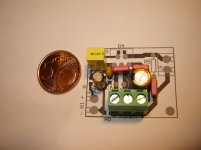
All capacitors are pin ptiched now 😀 Here is also a picture of elements on paper just to give you the idea how small this is(the board size is 40mm x 32mm). AndrewT can you please can you please confirm if the Cf=220pF and Rf=2.2k ratings are right.
Regards Aleš
p.s. Thank you ratza!
Regards Aleš
p.s. Thank you ratza!
Attachments
- Status
- Not open for further replies.
- Home
- Amplifiers
- Chip Amps
- lm1875 pcb layout for gainclone.