Back a while ago linuxguru posted a unity-gain buffer circuit that had some interesting features. See http://www.diyaudio.com/forums/anal...iscrete-opamp-open-design-94.html#post3164879
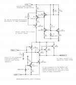
I studied it and began some investigations as to how its performance (already exemplary for such a simple circuit) might be improved. I mentioned I would eventually get around to posting something. I had occasion to revisit and extend that work recently while looking into an I-V converter that needed a buffer. A schematic of an example is attached.
One of the things I most like about linuxguru's approach is the notion that the JFET input device(s) are basically running the show, but with the heavy lifting into loads done by the rest of the circuitry. Not only is the noise performance outstanding, with a little care mostly due to the JFET(s), but the latter operate at both nearly constant voltage and constant current --- that is, constant dissipation. So the sorts of second-order effects that often plague designs that look otherwise good "on paper" are sidestepped here.
Quite a few more parts than the original, but I think worthwhile. The particular example will drive +/- 20V peak to peak into 600 ohm loads. I have yet to build it, and note the caveats about a propensity to high-frequency oscillations involving one or more active devices. I'd recommend actually stacking the three BF862 in the Z plane as it were, using a bit of bus wire as a combination conductor and heatsink for the gate leads.
The +50V is a constraint from other parts of associated circuits, and can be reduced for other applications, as long as the positive output swing is accomodated. The surface mount DMOS needs to have some copper in the vicinity of the large drain lead connection to manage the dissipations. The circuit needs a little lumped input C for ideal frequency response, which may well be supplied by the source impedance.
Attachments
guide to the possibly perplexed
The correspondence between the presented circuit and the original may be somewhat obscured.
Q7 through Q11 are just forming a low-noise high power-supply-rejection ~39mA current source, a function performed in the original circuit by J2 and R2. This could probably be simplified without much loss of performance.
Q3 and neighboring parts are another current generator, and substitute for R2 in the original. The effect of the generator is much higher gain of the loop that detects changes in the output current and stabilizes things. Of course the input impedance at the gate of Q2 is quite high.
There is no great effort made in this circuit by itself to stabilize output voltage drift, as in the intended application of buffering the resistor-terminated output of a current conveyor, there will likely be an overall d.c. servo. However as remarked elsewhere the voltage drift of BF862 parts is fairly small near Idss. If it were to be further stabilized, a matched set or a single matched device could be used to control a current generator that would replace Q7 etc.
Note that the gate-source voltage drift of Q5 is a second-order effect, since the output conductance at the 862 drains is fairly small.
The correspondence between the presented circuit and the original may be somewhat obscured.
Q7 through Q11 are just forming a low-noise high power-supply-rejection ~39mA current source, a function performed in the original circuit by J2 and R2. This could probably be simplified without much loss of performance.
...
If it were to be further stabilized, a matched set or a single matched device could be used to control a current generator that would replace Q7 etc.
Thanks, Brad - your circuit elaborations are always very illuminating.
For the upper current source, how about a set of 3x BF862 (matched to the lower 3) in parallel, with their gates tied to source, and a depletion-mode Supertex DMOS nFET (or similar) as an upper cascode for all 3 JFETs? That should take care of both the Vds (breakdown) of the BF862s and PSRR.
That sounds like a very acceptable approach, and would eliminate some parts.Thanks, Brad - your circuit elaborations are always very illuminating.
For the upper current source, how about a set of 3x BF862 (matched to the lower 3) in parallel, with their gates tied to source, and a depletion-mode Supertex DMOS nFET (or similar) as an upper cascode for all 3 JFETs? That should take care of both the Vds (breakdown) of the BF862s and PSRR.
By this point in most circuits, we are usually out of the woods with respect to noise anyway, so my concern for the output noise induced by a noisy current generator will usually be unwarranted.
One of the applications of this stage could be as the unity-gain buffer in Sallen-Key filter sections, ones which would typically use opamp voltage followers. Doug Self spends a good deal of time stressing the importance of characterizing opamps for input common-mode distortion, in his book on active crossover networks, a book I have yet to acquire but was able to get some of the content from in online excerpts.
It's interesting that with higher source impedances, for example 10k, it appears that the primary distortion mechanism is the variable input capacitance of the PMOS input device. The distortion predicted thus is still quite benign, but to reduce it further an additional BF862 can preface the PMOS gate, while sharing the drain connections of the other JFETs (a while back I also tried cascoding the PMOS drain, but it seemed intractable to stabilize). Additional current from the upstairs generator is needed, and a current gen for the new source as well. With a 10k resistive source and the added FET, about 2pF is needed to common at the new JFET gate to assure stability against oscillations. The circuit bandwidth looks to be -3dB at about 14MHz under those conditions.
I really do like this approach though. It appears to me hard to beat by anything else I've seen out there, including diamond buffers of various varieties. The adaptation to different loads with little change in performance is particularly appealing.
By this point in most circuits, we are usually out of the woods with respect to noise anyway, so my concern for the output noise induced by a noisy current generator will usually be unwarranted.
Another idea (not really novel) for the upper current source - instead of a somewhat hard-to-find depletion-mode MOSFET, perhaps a jelly-bean LM317 or similar could be put to use as the upper cascode element. It does have a small additional current component through the ADJ pin, but that should be fairly small compared to the 3 x Idss of the JFETs, and will contribute only a small additional offset voltage at the output (which in any case can be taken care off by an outer DC servo).
Of course, it would help if that ADJ current is relatively constant and independent of the input voltage to the LM317.
I wonder if anyone has ever looked at the noise in the 317 adjust terminal current? The noise of the device as such used as a regulator is almost certainly strongly dominated by the bandgap reference, so it's possible not too much attention was given to the adjust input current.
I'll be learning more, empirically, about 862 voltage drift soon, as I'm to the breadboard point with a composite amplifier using one 862 and an LME49990. There is a lot of d.c. gain and a servo is essential --- but the question is, once the JFET bias is adjusted at operating temperature for roughly zero volts out of the servo, how much servo range is really needed to assure that it never becomes unable to correct the main amplifier?
In a more extravagant design I've considered a Peltier device, and even stabilizing at a cooler temperature. But this invites issues with condensation if carried too far. The noise advantages are slight unless the impedances are super high, like in a charge amplifier.
Link (for future reference) to a Kaneda discrete opamp variant which borrows some ideas from the CCB for the output stage:
http://www.diyaudio.com/forums/anal...screte-opamp-open-design-297.html#post3626279
In principle, the VAS could use PMOS devices to improve the output swing capability, and the output stage could use NMOS devices like the 2N7002. With biasing changes, the LTP active load could also be PMOS - thus allowing an all-FET discrete opamp topology.
Last edited:
Link (for reference) to a thread about a Class-A push-pull BJT buffer (by Ken Peter and Elvee) which uses related ideas derived from the c.1973 Taylor source-follower, which in turn is derived from the c.40s White follower:
http://www.diyaudio.com/forums/soli...-buffer-power-output-stage-6.html#post2043894
(The clipping behaviour is a bit messy in simulation, but seems to scale well from mA to A of output-stage Iq.)
http://www.diyaudio.com/forums/soli...-buffer-power-output-stage-6.html#post2043894
(The clipping behaviour is a bit messy in simulation, but seems to scale well from mA to A of output-stage Iq.)
Last edited:
I'm beginning to look favorably on "quasi-complementary" stages lately, especially if an overall power amp has a bridge output. The efforts made chasing complementarities in P and N devices, whether bipolar or FET, just seem to be ultimately limiting. Of course local error correction usually helps a lot.Link (for reference) to a thread about a Class-A push-pull BJT buffer (by Ken Peter and Elvee) which uses related ideas derived from the c.1973 Taylor source-follower, which in turn is derived from the c.40s White follower:
http://www.diyaudio.com/forums/soli...-buffer-power-output-stage-6.html#post2043894
(The clipping behaviour is a bit messy in simulation, but seems to scale well from mA to A of output-stage Iq.)
I would like to see what Hansen is doing --- as I may have remarked, he believes he has single-handedly resurrected the diamond circuit for an output stage. Naturally the Stereophile writer doesn't know otherwise and dutifully reports this.
revisiting the revisited
With unity-gain buffers a topic elsewhere, I went back and reviewed the proposed design from the first post here, looking at reducing the distortion arising from variable input capacitance, which becomes important for high source impedances. Having looked at such a metric for a more conventional bootstrapped-cascode source follower and using 100k as the source impedance, including one approach to compensating for output loading, I went back to see how the linuxguru buffer was doing at 100k.
The answer is, not bad at all. But it dawned on me that I had never tried driving the P channel input device from the output, the sources of the BF862s.
It works a lot better that way, with some small changes in the input capacitance. About half a pF is needed to avoid peaking. I also changed the NPN current sink with the LED bias to a JFET with a bit of external source resistance, using a 2SK117, and this may very slightly degrade overall loop gain.
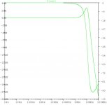
For a 10V peak input at 1kHz, with the generator driving 100k in, and the output driving 600 ohms, sims predict that most of the distortion arises at the input: to 15th harmonic, about 114ppb (0.114ppm); the distortion at the output is about 148ppb. Again thermal distortion in the 862s will be very small, as they operate at virtually constant power dissipation.
Worth building I think, to see how close one comes to these predictions. I might run some similar sims with ~SK170 parts. Although they are not likely as good as the 862s they are much easier to breadboard with.
Brad
With unity-gain buffers a topic elsewhere, I went back and reviewed the proposed design from the first post here, looking at reducing the distortion arising from variable input capacitance, which becomes important for high source impedances. Having looked at such a metric for a more conventional bootstrapped-cascode source follower and using 100k as the source impedance, including one approach to compensating for output loading, I went back to see how the linuxguru buffer was doing at 100k.
The answer is, not bad at all. But it dawned on me that I had never tried driving the P channel input device from the output, the sources of the BF862s.
It works a lot better that way, with some small changes in the input capacitance. About half a pF is needed to avoid peaking. I also changed the NPN current sink with the LED bias to a JFET with a bit of external source resistance, using a 2SK117, and this may very slightly degrade overall loop gain.
For a 10V peak input at 1kHz, with the generator driving 100k in, and the output driving 600 ohms, sims predict that most of the distortion arises at the input: to 15th harmonic, about 114ppb (0.114ppm); the distortion at the output is about 148ppb. Again thermal distortion in the 862s will be very small, as they operate at virtually constant power dissipation.
Worth building I think, to see how close one comes to these predictions. I might run some similar sims with ~SK170 parts. Although they are not likely as good as the 862s they are much easier to breadboard with.
Brad
Coming soon.Brad sounds interesting-gotta schematic handy?
...But it dawned on me that I had never tried driving the P channel input device from the output, the sources of the BF862s.
I believe Steven's version uses this idea, but with a PNP driving an NPN lower element. The minor problem with that is that it fixes output JFET Vds at about 0.6V - using a PMOS may give a bit more headroom for Vds. A commodity PMOS device like BSS84 may be workable, I'll check it in simulation in due course.
With a low-Z input, I found that I need R1-C1 to tame the peaking at the output. With the peaking tamed, it does give lower THD20 as shown, than with the PMOS gate cantilevered from the input. Simplified schematic below:
Attachments
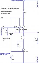
Yes, some compensation is required for low-Z inputs. It seems like a C to common at the input is pretty tractable. Also probably a small resistor in series with the output to a significant capacitative load is advised.With a low-Z input, I found that I need R1-C1 to tame the peaking at the output. With the peaking tamed, it does give lower THD20 as shown, than with the PMOS gate cantilevered from the input. Simplified schematic below:
schematic
Here is a schematic for a buffer that can drive up to the Idss of Q1, in this case about 10mA. A little less heroic than the paralleled BF862s but still excellent performance predicted---and a lot easier to breadboard.
Brad
Here is a schematic for a buffer that can drive up to the Idss of Q1, in this case about 10mA. A little less heroic than the paralleled BF862s but still excellent performance predicted---and a lot easier to breadboard.
Brad
Attachments
There is an instability, a couple of oscillatory bursts of several cycles at about 900kHz, predicted for big overloads (20V peak, 40V p-p) in the positive half of the waveform near the peak, which is due to the Boxall-Aldridge-style current source instability. If the positive rail is raised to 30V and R1 to 26.1k it goes away. An unlikely input signal, but the fix seems robust.Here is a schematic for a buffer that can drive up to the Idss of Q1, in this case about 10mA. A little less heroic than the paralleled BF862s but still excellent performance predicted---and a lot easier to breadboard.
Brad
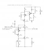
What I was concerned about when I looked at the circuit: the possibility under fault conditions of exceeding the gate-source breakdown voltage of the ZVN2106, or other NMOS part there. It seems not to be an issue, but belt and suspenders caution would provide a small diode to a biased zener spacing off of the negative rail.
- Status
- This old topic is closed. If you want to reopen this topic, contact a moderator using the "Report Post" button.
- Home
- Source & Line
- Digital Source
- linuxguru buffer redux and beyond