I recently came about the I/V circuit proposed by ESS's ES9039pro datasheet. Firstly let's show it here:

I will try to describe how I think it works, let's see how many misconceptions I have about it...
")
I will try to describe how I think it works, let's see how many misconceptions I have about it...
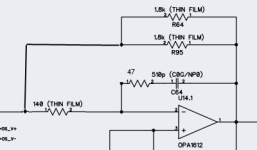
- There is a "deglitching" cap (C18.1) directly around the DAC outputs. I remember that this might cause problems with I/V opamp stability. Why is this suddenly not the case anymore? I see it's benefits, forming a 1st order low pass with the DAC output resistance (I calculated a cutoff of around 200kHz with 2x744 ohm output resistance of a single DAC output).
- U14.1/14.2 with their feedback components from the output to the inverting inputs form a "standard" opamp I/V circuit.
- U15/C72/R102 make an integrator with cutoff of about 2.6kHz, taking it's input from the summed I/V output (by R100/101), seeing only common mode voltage of the I/V outputs at it's inverting input. U15 noninverting input is referenced to ground.
- I/V opamps U14.1/U14.2 have a positive gain of ~744 on their noninverting inputs (R14/15/17/18) where the output of the servo is amplified.
- Where does the servo cutoff of 2.6kHz come from? Are frequencies between 2.6kHz and the edge of the audio band (20k) of lesser importance?
- Why is the servo output amplified by 744 and then works as a reference for the I/V opamps?
One more question:
The benefit shall be that the common mode currents produced by the DAC chip, which si then converted to common mode voltage at the outputs ov the I/V opamps is then canceled out by feeding it back to the noninverting inputs of the I/V opamps. Is that correct? If so, why is there a gain necessary (question 2 alsready partly asks that)?
The benefit shall be that the common mode currents produced by the DAC chip, which si then converted to common mode voltage at the outputs ov the I/V opamps is then canceled out by feeding it back to the noninverting inputs of the I/V opamps. Is that correct? If so, why is there a gain necessary (question 2 alsready partly asks that)?
I recently came about the I/V circuit proposed by ESS's ES9039pro datasheet. Firstly let's show it here:
View attachment 1155146
I will try to describe how I think it works, let's see how many misconceptions I have about it...
- There is a "deglitching" cap (C18.1) directly around the DAC outputs. I remember that this might cause problems with I/V opamp stability. Why is this suddenly not the case anymore? I see it's benefits, forming a 1st order low pass with the DAC output resistance (I calculated a cutoff of around 200kHz with 2x744 ohm output resistance of a single DAC output).
I think that the phase lead caused by C64 and C68 is supposed to keep the loop stable, provided the op-amps can handle large capacitive loads when working at a gain of -2 * C18.1/C64. For differential signals at sufficiently high frequencies, C64, C68 and C18.1 form a frequency-independent voltage divider.
My questions:
- U14.1/14.2 with their feedback components from the output to the inverting inputs form a "standard" opamp I/V circuit.
- U15/C72/R102 make an integrator with cutoff of about 2.6kHz, taking it's input from the summed I/V output (by R100/101), seeing only common mode voltage of the I/V outputs at it's inverting input. U15 noninverting input is referenced to ground.
- I/V opamps U14.1/U14.2 have a positive gain of ~744 on their noninverting inputs (R14/15/17/18) where the output of the servo is amplified.
Looking forward to your answers, as always
- Where does the servo cutoff of 2.6kHz come from? Are frequencies between 2.6kHz and the edge of the audio band (20k) of lesser importance?
- Why is the servo output amplified by 744 and then works as a reference for the I/V opamps?
Question 1: I think C72 is chosen as small as possible without compromising feedback loop stability. I don't know what the purpose of R102 is.
Question 2: I guess the positive feedback via R15 and R17 is some kind of trick to reduce the effect of finite op-amp gain on the differential input impedance, but that is really just a guess.
Well, this is a fully differential OpAmp made from standard OpAmps and with the advantage of access to fine-tuning (besides the potential "unique/special part" availability issue with integrated FDAs, designers are more aware to this by now).Anyhow I don't see the point of this circuit. Differential stage (e.g. using OPA1632) instead of the integrator should work fine.
Note the small positive feedback which establishes a slightly negative input impedance. Speculation from my side, it could be to compensate for actual metal-mask and bonding wire resistances or maybe it just an empirical patch to improve specs.
Yes, a known re-balancer circuit and basically the only way to level-shift a unity-gain buffer, at the cost of lowish input impedance and AC-coupling.
When some gain (>=2 or so, practically) is allowed for, a true high impedance and DC-coupled re-balancer can be made injecting the correction signal into the inverting node, with the servo amp now running non-inverting (and thus with different compensation).
In general, I found intuitive to be circuit function, it's a composite amp with the servo being the master and the I/V-amps being slaves in a constant closed-loop gain arrangement and simply paralleled.
The role of R102 is indeed unclear, an "Angst" resistor of sorts but maybe it does something useful.
The role of R102 is indeed unclear, an "Angst" resistor of sorts but maybe it does something useful.
The last paragraph of chapter 2.3 in AES6455 sums it up quite nicely.ADC input buffer circa 1997.
BTW, the proposed circuit for the ES9027pro is also, let's say, interesting:

Basically the same idea of a full-frequency CM servo, but...
... why is the reference for the bottom I/V taken from the feedback node of the top I/V? It will work but it also should have more distortion -- and maybe that's the trick, some sort of compensation going on? Or is it simply a drawing error?
Also, the high differential RF noise gain from the 100pF vs 2.2nF feedback looks suspicious.
The reference nodes for the I/Vs is a mix of (mainly) the CM-servo's output and (a very small part of) the individual I/V's output. This creates a very slightly negative input impedance at audio frequencies. The concept is well known when using transformer inputs in current mode ("zero field" mode), to cancel the DC winding resistance of the transformer, see https://www.lundahltransformers.com/wp-content/uploads/datasheets/6404.pdfCould you please explain where the "small positive feedback" cones from?
Now I see, what I misrepresented as gain for the servo voltage is in fact a resistor divider between the output of the opamp (high value, low contribution to positive feedback) and the servo output (low value, high contribution)The reference nodes for the I/Vs is a mix of (mainly) the CM-servo's output and (a very small part of) the individual I/V's output. This creates a very slightly negative input impedance at audio frequencies.
Why does the mechanism only work at audio frequencies and generate negative input impedance there?
I want to adapt this circuit to the ES9038Q2M in mono mode which then has a combined output resistance of 387 ohms. Is it OK to simply scale down caps by a factor of roughly 2? I.e. C18.1 => 1nF, C64/C68 => 270pF. The I/V feedback resistors, now 950 ohms would need to be scaled up by a factor of two, i.e. 1.8k.
What if I want lower output voltage from the I/V and want to significantly scale down the I/V resistors (in the range of 500 to 1000 ohms), do I need to adjust C64 and C68?
I was planning to use this kind of active lowpass filter after the I/V which doubles the output voltage anyway. So we were shooting for a I/V feedback resistor of 500 ohms, to give 2.7V RMS after the I/V and 5.4V RMS after the LP. makes sense?

Why 887 ohms? We have lots of these laying around
Why 887 ohms? We have lots of these laying around
- Home
- Source & Line
- Digital Line Level
- Let's talk about the I/V circuit with common mode servo as shown by ES9039pro datasheet