Sorry for my last post, It vas late 
How do you get the result that the max power i the output devises are at ½ railvoltage out?
\Jens
How do you get the result that the max power i the output devises are at ½ railvoltage out?
\Jens
I am in principle fine with the methodology. My hesitation comes from my view that since the Vbe of the driver and the output devices is likely to behave different from the Vbe of the bias transistor or the forward voltage of the diodes. For example, a 1 degree temperature rise on the mj3281 may cause more or less voltage drop than the same temperature rise on a tip41, or 2n5550, or a 1n4148/1n4001.
However, if you think that the largest Vbe impact will come from the output devices, it makes more sense to use the same transistor as a Vbe multiplier, 🙂, rather than dioades or other transistors.
However, if you think that the largest Vbe impact will come from the output devices, it makes more sense to use the same transistor as a Vbe multiplier, 🙂, rather than dioades or other transistors.
Jens, maximum power dissipation is at 1/3 of full power (class B stage) , assuming ideal parts.
I can't deliver a formula, too tired for this but there was a good article in JAES some time ago with total "genomgång(*)" of the subject and all Class A, B, AB etc.
(*) missing the english of "going through all facts".
I can't deliver a formula, too tired for this but there was a good article in JAES some time ago with total "genomgång(*)" of the subject and all Class A, B, AB etc.
(*) missing the english of "going through all facts".
peranders said:Jens, maximum power dissipation is at 1/3 of full power (class B stage) , assuming ideal parts.
I can't deliver a formula, too tired for this but there was a good article in JAES some time ago...
As Millwood pointed out, for DC the maximum power dissipation in the output stage for class B occurs when the load voltage is Vcc/2. For this case, the maximum power dissipation is Vcc*Vcc/(4*RL).
For the sine wave case into a resistive load, the maximum power disspation occurs when the peak load voltage is 2*Vcc/pi. For that case, the power dissipation in the output stage is Vcc*Vcc/(pi*pi*RL).
"he power dissipation in the output stage is Vcc*Vcc/(pi*pi*RL)"
As I know this formula is:
Pdmax=Vcc^2/(2pi^2*RL)=Vcc^2/(Rl*0.2027)
The result is the whole dissipation of the output stage.
Sajti
As I know this formula is:
Pdmax=Vcc^2/(2pi^2*RL)=Vcc^2/(Rl*0.2027)
The result is the whole dissipation of the output stage.
Sajti
sajti said:"he power dissipation in the output stage is Vcc*Vcc/(pi*pi*RL)"
As I know this formula is:
Pdmax=Vcc^2/(2pi^2*RL)=Vcc^2/(Rl*0.2027)
The result is the whole dissipation of the output stage.
Sajti
Ooops I made a mistake:
The right formaula:
Pdmax=Vcc^2/(2pi^2*RL)=0.2027*Vcc^2/(RL)
Sajti
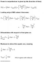
I didn't follow andy's notation closely. But there is a much simpler way to figure the maximum average power dissipation on the devices in half cycle (assuming perfect devices).
the peak drop on the load R is Vcc (rail voltage). so the RMS value of output voltage is Vrms=Vcc/sqrt(2), and RMS current is Irms=Vcc/(sqrt(2)*R). and the power dissipation on the load is Pl=Vrms*Irms=Vcc^2/(2R).
from the power supply's point of view, it is providing a steady rail voltage of Vcc, and a sine current whose RMS is Irms=Vcc/(sqrt(2)*R). so total power provided by the power supply is Pr=Vcc*Irms=Vcc^2/(sqrt(2)*R).
the difference between Pr and Pl, Pr-Pl=Vcc^2/R(1/sqrt(2)-1/2)=Vcc^2/R*(sqrt(2)-1)/2=0.207*Vcc^2/R, very close to sajti's figure.
Note that this is the AVERAGE power dissipation on the output device. At some point, power dissipation on the device can be higher or lower than this figure - Jens and I provided the true Maximum power dissipation that the device may have to dissipation at an instant, not an average.
If you size your heatsink with the calculated figure above, and you feed the amp with a low-frequency signal (like a DC signal), the amp may overheat.
sajti said:
Ooops I made a mistake:
The right formaula:
Pdmax=Vcc^2/(2pi^2*RL)=0.2027*Vcc^2/(RL)
Sajti
I believe 1/(2*pi^2)=1/(2*3.1415^2)=1/(2*9.869)=1/19.738=0.0507.
you arrived at the right figure but your formula didn't work out correctly.
another note for andy.
you don't really need to calculate so meticulously the power dissipation on the output devices for this excercise.
Basically, the power dissipation on the output devices is
Po=V*I. and for a BJT, the base current Ib=I/beta. And Ib happens to be the emitter current for the driver. and the voltage drop on the driver is just one Vbe away from that of the output devices - Vbe of the output devices for an EF design.
so the power dissipation on the driver is
Pd=(V-Vbe)*Ib ~=V*I/beta=P/beta.
That is, the power dissipation on the driver is 1/beta'th of that on the output devices.
millwood said:
I believe 1/(2*pi^2)=1/(2*3.1415^2)=1/(2*9.869)=1/19.738=0.0507.
you arrived at the right figure but your formula didn't work out correctly.
I made a huge mistake

 0.2027=2/pi^2
I use this formula long time ago, but I learned in the high school so I dindn't remember exactly the source of it.
The Pdmax=0.2*Vcc^2/RL is sure, I planned the heatsinks for all my amplifier with this figure, and all works properly

My current project will use 4pairs of MJL21193/94 with regulated +/-40V. The dissipation will be 5W/device with 8ohms, and 10W/device with 4ohms.
Sajti
"That is, the power dissipation on the driver is 1/beta'th of that on the output devices"
And what about the bias current and dissipation? In my current project the drivers run with 100mA bias. With Vcc=40V, it will be 4W without any output signal. My output devices will dissipate 40W (20W for NPN), in this case one of my driver will heat with 4W+20W/60=4.333W
If I plan the heatsinks for the dissipation with Your figure, I will simply burn out my drivers
Sajti
sajti said:
I made a huge mistake
(...)
The Pdmax=0.2*Vcc^2/RL is sure, I planned the heatsinks for all my amplifier with this figure, and all works properly
This sounds like your numbers and mine are making sense now. I wasn't careful about defining which power dissipation I was referring to. My formula is for half of the output stage. So to get the dissipation in a single transistor, you would divide my number by the number of output transistors in parallel - two for the Leach amp. It looks like yours is for the whole output stage, so for the Leach amp you would divide by 4 to get the dissipation per transistor - giving the same result.
sajti said:And what about the bias current and dissipation?
Sajti
Sajti, I did not consider the impact of biasing on pre-driver power dissipation - most of my circuitry is in class B (class AB by everyone else). so if you have large bias in the pre-driver, the forumula I gave wouldn't work.
Re: Bias diodes
Hi, people
The diodes need to sense the temperature of all output devices.
From Low Tim Amp FAQ:
http://users.ece.gatech.edu/~mleach/lowtim/faq.html
Q: "Can I mount each power transistor on separate heat sinks?"
A: " Don't do this. The amplifier will not be thermally stable. The four bias diodes should see the average temperature of all four output transistors. This occurs only when all transistors and all bias diodes are on the same heat sink. There is an exception. You can mount the two NPN output transistors for one channel on one heat sink and the two PNP output transistors on another. Either put all four bias diodes on one of the heat sinks or put two bias diodes on each.
I once had a student who used 2 heat sinks per channel with two output transistors on each, a NPN and a PNP. He put the bias diodes on only one of the heat sinks. His amp was thermally unstable. The heat sinks without the diodes overheated. Putting both NPNs on one heat sink and both PNPs on the other solved the problem. "
Hi, people
JensRasmussen said:
I mounted my diodes on an output transistor because the heatsink weighs 7 kg, and therefor will so long to heat, that output devices are in danger of overheating before the protection circuit ever finds out the amp is hot.
The diodes need to sense the temperature of all output devices.
From Low Tim Amp FAQ:
http://users.ece.gatech.edu/~mleach/lowtim/faq.html
Q: "Can I mount each power transistor on separate heat sinks?"
A: " Don't do this. The amplifier will not be thermally stable. The four bias diodes should see the average temperature of all four output transistors. This occurs only when all transistors and all bias diodes are on the same heat sink. There is an exception. You can mount the two NPN output transistors for one channel on one heat sink and the two PNP output transistors on another. Either put all four bias diodes on one of the heat sinks or put two bias diodes on each.
I once had a student who used 2 heat sinks per channel with two output transistors on each, a NPN and a PNP. He put the bias diodes on only one of the heat sinks. His amp was thermally unstable. The heat sinks without the diodes overheated. Putting both NPNs on one heat sink and both PNPs on the other solved the problem. "
?
I mounted my diodes on an output transistor because the heatsink weighs 7 kg, and therefor will take so long to heat, that output devices are in danger of overheating before the protection circuit ever finds out the amp is hot.
This does not mean that the output transistors are on different heatsinks
\Jens

My leach files
Here are the files for my LEACH amp.
You schould change the resistorvalues to the original if you want the original. Also the components around the NFB must be changed.
Note that I have used BC transistors in the layout. They are not pin- compatible with the original types.
Have fun
I'm interrested in seeing the results when they are ready
\Jens
Attachments
- Status
- Not open for further replies.
- Home
- Amplifiers
- Solid State
- Leach amp bias diodes