This is a cross post, as I asked this question at the other place, but they are a bit reserved at the moment and I need to send in my layout, to get my boards when I am on vacation.
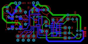
In the attached pic with the schematic the Dac has two pins (17 and 18) right next to each other that are suppose to be tied to the 5V supply.
Each of them seems to need a separate 0.1uf decoupling cap.
Why is it necessary to do that since they are just 2mm apart?
Do I get by with just one cap like on my layout in the pic?
If someone sees any other flaw in the layout, please feel free to command on it.
Greets,
Klaus
Attachments

Hello,
I can\t really comment on the pcb design, I don't have the experience.
What is the digital source for this DAC? From where do you get the I2S signal?
I can\t really comment on the pcb design, I don't have the experience.
What is the digital source for this DAC? From where do you get the I2S signal?
Since it's in the datasheet schematic, put in the caps. I'm guessing that the sigma-delta portion of this DAC creates a decent amount of noise, hence the need for additional filtering.
- Status
- Not open for further replies.