Hi all,
I recently made some stereo TDA7293 boards and am now working on a Rev.B because I realise, in hindsight, that my grounding topology is not particularly great (this is unrelated to my previous post about hum). One constraint I face in particular is that, for reasons of space and packaging, I need to build multi-channel (at least 2ch) boards and I have no more than 50mm of PCB width available for each channel. Most of the small-signal stuff is SMD, so that helps a little.
One major problem I have is no means to measure distortion with any accuracy so I am somewhat working in the dark with respect to trying different topologies that I've seen people recommend. A couple of features in particular I have seen on other power amp boards are:
An example of items 2 and 3 is in this LM3886 design, where there are separate PGND and SGND cables to each channel PCB. Implicitly also item 4 because it uses a separate board for each channel.
However, no commercial amp kits I've built - nor appnote PCB layouts - seem to take the approach of items 2, 3 or (where stereo) 4. Just one PGND from the reservoirs to an amp PCB, and the speaker return also goes via the PCB which ensures that the loop area in the output is minimised.
Further wrinkles:
With a TDA7293, it should be possible because there are separate supply pins on the chip... but I have not seen any published/tested designs that utilise the separate power pins in this way. Everyone, including the appnote, seem to just tie them together with a bit of copper. The appnote does have its "high efficiency" design but that's just Class G; at high power levels, the same half-wave noise on PWVs will appear on Vs.
I was considering putting a diode from PWVs to Vs and a decent decoupling cap on Vs (to where?!), on the principle that that should hold up Vs through any ripple on PWVs. But I don't know how to size the cap without knowing the current draw on Vs pins, and am concerned that I will just make it worse because the current through that diode might get mighty discontinuous - I would be trading some probably irrelevant third harmonics for much higher harmonics on the Vs pins, at some reduced level, and for which I have no idea of the PSRR at either frequency. As above, I do not have the equipment to do an A/B comparison. I don't really have the space to do a whole separate PSU for the input stages either, which would avoid that problem.
The reference design does not use hum-break resistors, and doesn't say what the SGND pin actually does. Should it be a stable local voltage reference? Should it align with the local system ground, or should it follow the virtual ground in the feedback network? What should the relationship between SGND and HBR be?
In terms of the speaker returns, I can see the benefit of not having a small copy of your output signal appear in PGND due to wire impedance, doubly so in terms of cross-talk on a multi-channel PCB. However, does it really matter if that noise on PGND is present if the whole amplifier feedback loop and ground reference are independent of PGND due to a separate SGND run? Yes there's direct cross-talk in the outputs from the shared PGND cable (200mm of 2.5mm^2 => 1.4mR => -75dB into 8R?) but that should be about it?
Therefore, I have a whole bunch of questions:
You opinions please on the various combinations of options? Especially if you have any experience with interesting power-supply topologies for the TDA7293 and its behaviours.
thanks...
I recently made some stereo TDA7293 boards and am now working on a Rev.B because I realise, in hindsight, that my grounding topology is not particularly great (this is unrelated to my previous post about hum). One constraint I face in particular is that, for reasons of space and packaging, I need to build multi-channel (at least 2ch) boards and I have no more than 50mm of PCB width available for each channel. Most of the small-signal stuff is SMD, so that helps a little.
One major problem I have is no means to measure distortion with any accuracy so I am somewhat working in the dark with respect to trying different topologies that I've seen people recommend. A couple of features in particular I have seen on other power amp boards are:
- separate supplies including separate ground and separate decoupling caps for the input stages
- running the input-stage ground (SGND) back to the PSU star separately from power ground (PGND) on the PCB
- running the speaker return back to reservoir/star GND instead of to the PCB PGND
- running separate PGND lines for each channel, from the reservoirs to the output-stage decoupling centres
An example of items 2 and 3 is in this LM3886 design, where there are separate PGND and SGND cables to each channel PCB. Implicitly also item 4 because it uses a separate board for each channel.
However, no commercial amp kits I've built - nor appnote PCB layouts - seem to take the approach of items 2, 3 or (where stereo) 4. Just one PGND from the reservoirs to an amp PCB, and the speaker return also goes via the PCB which ensures that the loop area in the output is minimised.
Further wrinkles:
- The TDA7293 has four power pins, one pair for the input/driver stage, and one pair for the output stage.
- I am slightly puzzled about decoupling in that LM3886 link above, wherein there are no decoupling caps attached to SGND
With a TDA7293, it should be possible because there are separate supply pins on the chip... but I have not seen any published/tested designs that utilise the separate power pins in this way. Everyone, including the appnote, seem to just tie them together with a bit of copper. The appnote does have its "high efficiency" design but that's just Class G; at high power levels, the same half-wave noise on PWVs will appear on Vs.
I was considering putting a diode from PWVs to Vs and a decent decoupling cap on Vs (to where?!), on the principle that that should hold up Vs through any ripple on PWVs. But I don't know how to size the cap without knowing the current draw on Vs pins, and am concerned that I will just make it worse because the current through that diode might get mighty discontinuous - I would be trading some probably irrelevant third harmonics for much higher harmonics on the Vs pins, at some reduced level, and for which I have no idea of the PSRR at either frequency. As above, I do not have the equipment to do an A/B comparison. I don't really have the space to do a whole separate PSU for the input stages either, which would avoid that problem.
The reference design does not use hum-break resistors, and doesn't say what the SGND pin actually does. Should it be a stable local voltage reference? Should it align with the local system ground, or should it follow the virtual ground in the feedback network? What should the relationship between SGND and HBR be?
In terms of the speaker returns, I can see the benefit of not having a small copy of your output signal appear in PGND due to wire impedance, doubly so in terms of cross-talk on a multi-channel PCB. However, does it really matter if that noise on PGND is present if the whole amplifier feedback loop and ground reference are independent of PGND due to a separate SGND run? Yes there's direct cross-talk in the outputs from the shared PGND cable (200mm of 2.5mm^2 => 1.4mR => -75dB into 8R?) but that should be about it?
Therefore, I have a whole bunch of questions:
- Has anyone tried a separate regulated supply for +Vs/-Vs on a TDA7293? How much current is required?
- If you implemented such a regulated supply, would you decouple VS (pins 7&8) to SGND (pin 4) or to PGND?
- If I use a hum-break resistor, to which side of it is pin 4 (SGND on the chip) connected?
- If I run separate SGND and PGND cables to each board, is there any benefit to duplicating the PGND cables into one per channel, or running the speaker returns back directly to the star instead of via the PCB? Presumably there is no benefit to both splitting PGND intl LGND and RGND wires, and having the speaker returns not visit the board?
- Am I just chasing effects down below -90dB and should just stop worrying and be happy? 🙂
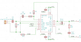
- 7293-a shows a single power supply (probably OK), no decoupling to SGND (correct I think), and with SGND/pin4 on the input side of the hum-break resistor (who knows; probably wrong?)
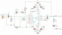
- 7293-b shows a split power supply using diodes (not sure), decoupled to SGND instead of PGND (probably wrong because of the diode, but maybe right if the Vs supplies were completely independent of the PWVs supplies) and with SGND/pin4 to actual SGND, with only the negative feedback path being on the input side of the HBR (who knows; probably right?).
You opinions please on the various combinations of options? Especially if you have any experience with interesting power-supply topologies for the TDA7293 and its behaviours.
thanks...
Attachments
Last edited:
Anyone? Bueller?
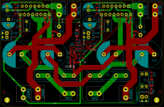
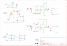
OK I totally get not wanting to wade through my wall of hypotheticals. Maybe someone with concrete experience in power-amp PCB layout can critique a screenshot of a specific proposal... I've got both options in there wrt hum-break resistor; one of them will be a 0R.
(ignore the stuff in the middle, it's just UNMUTE-control circuitry).


