Erratas
Hi ZM,
Long time no see
Double check, Spot one error:
B1 supply got to be higher than 24v to provide -17.8v for SIT gate.
This value needs to be adjusted for different SIT
Cheers
yup
mistake with grounds in drawing
3 most left ones , need to go to neg. supply
Hi ZM,
Long time no see
Double check, Spot one error:
B1 supply got to be higher than 24v to provide -17.8v for SIT gate.
This value needs to be adjusted for different SIT
Cheers
If I can so do you
you don't know me yet 😀
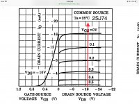
one exemple of my dumbiness : this amp must need some gain so do you think a simple single ended gain circuit with N channel Vfet 2SJ74 with -17V VDS direct coupled to the gate of the second stage would work ?
so we will need only one negative supply for the amp ?
Last edited:
Pink candle, haha, poor man lubricants for threading and bicycle chain.
That's what I thought. I would like to try myself! 🙂
It can be better than spilling the tapping oil.
I also remember that our old generation used the candle for sliding drawers.
I look forward to your progress with the circuit.

...a simple single ended gain circuit with N channel Vfet 2SJ74 with -17V VDS direct coupled to the gate of the second stage would work ?
so we will need only one negative supply for the amp ?
It should be P channel, you meant,
Sure it does work as a voltage amplifier for driving the pair SIT - Lateral buffer by providing a négatif 17.5v (this value was measured from my prototype).
But how well it is, i don’t know, haven’t got any P 2SJ74 fet at hand, only made a comment by looking at the 2SJ74 spec.
At 17.5 Vds, you have very little chance to create any H2 with negative phase.
Salut
Attachments
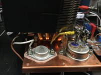
first stage the transistors are finally here.
to see if it can works i presume that i must check if at the Same VDS et IDS i'v got he same VGs on the quad chips ; is there a safe margin or it must be perfectly matched ? 🙂
Without Mr Pass and many contributors to the Pass Labs Forum, I wouldn’t have a clue what is concerning a class A SIT audio amplifier.
Those information helped me to build an SIT amp with a complementary lateral mosfet, my LATE - SIT
Nice work, Pascal!
Having patience
Step one:
Thermal test
Mount 4 beefy but cheapest mosfets to heatsink, the one intended for your project.
Connect drain-source to your power supply (30V/5A)
Connect gate-source to a variable 0-9v, adjust to 4A Ids
Heatsink must be within 50 degC at room ambiance’s 22degC
Step two:
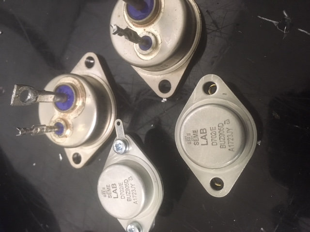
Mount 2 Sits and 2 Laterals to heatsink. (Precaution anti static, grounded soldering iron tip, temporarily shorted Sit gate-source).
Connect BUZ905D Drain-Source to 15V3A power supply
Adjust Gate-Source with 0-9V variable to reach 2A.
Lock and record the value of Vgs@2A
Connect BUZ905D and THF-51S according to the schéma.
Connect +30 to chassis and -30 to BUZ’s drain.
Connect BUZ’s gate-source to the locked variable 0-9V supply.
Connect Sit’ gat-source with a second variable 0-9V supply and adjust it until both transistors have an equal 15V Drain-Source.
Record that value.
Repeat for all transistors, to get all value Vgs, don’t have to match 100%, as close as you can get for left and right channels
Using correct amperage and colour coded electrical wire with idiot proof polarity connectors.
Don’t forget a Dubonnet for calming down your nerves
Cheers
first stage the transistors are finally here.
to see if it can works i presume that i must check if at the Same VDS et IDS i'v got he same VGs on the quad chips ; is there a safe margin or it must be perfectly matched ? 🙂
Step one:
Thermal test
Mount 4 beefy but cheapest mosfets to heatsink, the one intended for your project.
Connect drain-source to your power supply (30V/5A)
Connect gate-source to a variable 0-9v, adjust to 4A Ids
Heatsink must be within 50 degC at room ambiance’s 22degC
Step two:
Mount 2 Sits and 2 Laterals to heatsink. (Precaution anti static, grounded soldering iron tip, temporarily shorted Sit gate-source).
Connect BUZ905D Drain-Source to 15V3A power supply
Adjust Gate-Source with 0-9V variable to reach 2A.
Lock and record the value of Vgs@2A
Connect BUZ905D and THF-51S according to the schéma.
Connect +30 to chassis and -30 to BUZ’s drain.
Connect BUZ’s gate-source to the locked variable 0-9V supply.
Connect Sit’ gat-source with a second variable 0-9V supply and adjust it until both transistors have an equal 15V Drain-Source.
Record that value.
Repeat for all transistors, to get all value Vgs, don’t have to match 100%, as close as you can get for left and right channels
Using correct amperage and colour coded electrical wire with idiot proof polarity connectors.
Don’t forget a Dubonnet for calming down your nerves
Cheers
V2
V1 had been poorly designed for biasing the output transistors.
I used the trimpot of the DN2540 current regulator to change Vbias, that did affected the linearity of the driver due to current variation.
The V2 has separated V bias adjustment, no interference with Driver current that would move the DN2540 out of the square law corridor (70mA / 10Vds)
How does it works:
Upper DN2540 supplies 70mA as CCS to the lower DN’s with 22 Ohm source resistor.
That resistor will potentially different the gate by 1.5V, where the DN is behaving just like a triode but the output generates only positive H2
The Driver will bias and reverse its output to the power stage then assuming a voltage conversion to current will happen with a taste of H2 negative.
Cheers
Attachments
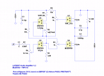
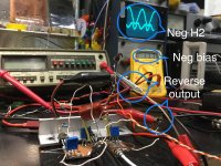
hi , pascal thanks for the test procedure. something i don't understand ( again 🙂 ) in the V2 schematic how the VFET and mosfet negative bias could be done with 32V positive supply ?
in the V2 schematic how the VFET and mosfet negative bias could be done with 32V positive supply ?
One never would understand why a negative bias can be done with a positive supply while standing on a negative ground of a positive supply.
One can see a negative bias of that same supply if he or she would stand on a positive ground (ie if you take that +32 as ground, you will see the bias output has a negative value)
When you finish the thermal test and all Vgs had been measured, we will run a third step.
Cheers
.
Attachments
one don't understand again how a 32V positive supply tie to ground could make a -17V bias with the second negative supply tie to ground .😕
one try to learn slowly 🙂
one try to learn slowly 🙂
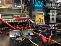
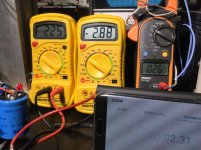
i have mesure this morning and i have for 2A IDS i have -2,4V VGS on the THF51S and -3,1V on the BUZ905D MOSFET ..
one will say i'm on the way to gave up ...😛
one will say i'm on the way to gave up ...😛
Last edited:
… ..
one will say i'm on the way to gave up ...😛
Once doubt begins, it spreads rapidly.
Waiting for you to pass the thermal test.
...
Waiting for you to pass the thermal test.
As an example
.
Attachments

Hi Pascal,
In your last circuit, the Source of THF and Drain of BUZ are connected. I checked your 1st circuit hand drawn in the picture, both Sources are connected. Which one is the one you are testing?
Like juanitox, I am still trying to understand the ground in your circuit....
In your last circuit, the Source of THF and Drain of BUZ are connected. I checked your 1st circuit hand drawn in the picture, both Sources are connected. Which one is the one you are testing?
Like juanitox, I am still trying to understand the ground in your circuit....
Lethal mistake
My bad
Deeply apologise to you and Juanitox.
Hi Pascal,
In your last circuit, the Source of THF and Drain of BUZ are connected. I checked your 1st circuit hand drawn in the picture, both Sources are connected. Which one is the one you are testing?
Like juanitox, I am still trying to understand the ground in your circuit....
My bad
Deeply apologise to you and Juanitox.
Attachments

i have mesure this morning and i have for 2A IDS i have -2,4V VGS on the THF51S and -3,1V on the BUZ905D MOSFET ..
one will say i'm on the way to gave up ...😛
Hope that your BUZ is still in good health.
Check your PM.
Cheers
.
Attachments

Power supplies
The 30V is for power stage, this value was selected due to 10000uF/35V capacitors have good value for money’s, about 1.6 au$/each shipped from China.
The 32V is for driver stage, I use 2 laptop batteries (4S2P x 2 lithium 3.7V element) for convenience until the sweet spot of DN2540 drain source voltage and current found, then a very low noise power supply will be built.
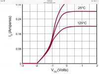
The spec shown 10Vds and Vgs -1 to -2, square law behavior.
Cheers
In the circuit, there are 32V and 30V supply. Are these separate supply?
The 30V is for power stage, this value was selected due to 10000uF/35V capacitors have good value for money’s, about 1.6 au$/each shipped from China.
The 32V is for driver stage, I use 2 laptop batteries (4S2P x 2 lithium 3.7V element) for convenience until the sweet spot of DN2540 drain source voltage and current found, then a very low noise power supply will be built.
The spec shown 10Vds and Vgs -1 to -2, square law behavior.
Cheers
Attachments
- Home
- Amplifiers
- Pass Labs
- LateSit