Re: BOMs
http://www.diyaudio.com/wiki/index.php?page=Building+guide
rjkdivin said:
I'm interested why it is important to maintain 47pf for C105 and C106 when it is listed as 33-330pf for the Jan BOM, 47pf for the Al BOM, and 390pf on the schematic? I'm not arguing with you....just curious! I must have missed some posts that discussed this value.
Was there ever a revised schematic posted for the Pinkmouse boards? All I have is Jan's schematic from the Delta Audio site. It doesn't even have C303/4 as far as I can tell.
Robert
http://www.diyaudio.com/wiki/index.php?page=Building+guide
Troy's e-mail = stgrab@yahoo.com
I will try to remember to post my latest BOM tonight when I get home. You can compare it to yours then.
All of the Links on my BOM are to the actual parts that have been tested and ordered for both revs of boards.
I'm glad you’re ordering your own because after this mess of sorting through the two DIFFERNT board sets I don't think I have enough patience to order and kit more channels for a second GB.
I did 99% of the research and TESTING for the parts. The BOM I have at home is good for anyone who wants to order their own parts.
Once I rx the last of the components and have had a chance to insert and test fit each one I will post the last BOM.
Cheap MJL's - should I be wary?
http://www.futurlec.com/
have MJL21193/4 for $2.90, from 'various' manufacturers.
Has anyone used this company? Any forgery issues with these devices?
thanks
http://www.futurlec.com/
have MJL21193/4 for $2.90, from 'various' manufacturers.
Has anyone used this company? Any forgery issues with these devices?
thanks
rjkdivin said:I'm interested why it is important to maintain 47pf for C105 and C106
C105 and C106 are local frequency compensation capacitors, there to add some phase margin, and that prevents overshoot and oscillation.
It's a Lead compensation, like the name says it "leads" the high frequency range.
The higher the value, the higher the phase margin, the less prone to instability the amplifier is.
But, it lowers the highest frequency, make them too large and high frequency reproduction suffers.
The ticket is to keep them as low as possible, but high enough to keep overshoot and oscillation under control.
The 390pF is an exceptional high value in that position and a questionable value in the published circuit diagram in the beginning of the thread.
The range of values was mentioned to enable individual experimentation.
Re: Re: BOMs
Yeah, what he said. Open the wiki and search for "c105" and you will find info about this.
bremen nacht said:
Yeah, what he said. Open the wiki and search for "c105" and you will find info about this.
jacco vermeulen said:
C105 and C106 are local frequency compensation capacitors, there to add some phase margin, and that prevents overshoot and oscillation.
The 390pF is an exceptional high value in that position and a questionable value in the published circuit diagram in the beginning of the thread.
Thanks Jacco....thats a great explanation! I did have a look at the posts referenced in WIKI, but was still unsure as to the function, and potential results of higher capacitances.
Robert
I recommended 47p as a good all round value after testing, safe for difficult loads and/or inexperienced constructors with no test gear. If you can properly test with your own speakers you might be able to drop this to 22p, but I don't advise this unless you know what you are doing.
Attachments
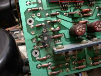
Re: my photo copy from
Whats the Story Nark?
nark said:
Whats the Story Nark?
Re: Re: my photo copy from
The owner was trying to burn-in the pre-amp with his Krell 50.
Krell 50 was overheated and blow up some parts.
K-amps said:
Whats the Story Nark?
The owner was trying to burn-in the pre-amp with his Krell 50.
Krell 50 was overheated and blow up some parts.
Re: Re: Re: my photo copy from
Or perhaps the owner had a one night stand with a Mark Levinson... The homey KSA-50 (who was a Mk. II herself) could not take it.
jajabin said:
The owner was trying to burn-in the pre-amp with his Krell 50.
Krell 50 was overheated and blow up some parts.
Or perhaps the owner had a one night stand with a Mark Levinson... The homey KSA-50 (who was a Mk. II herself) could not take it.
Re: Cheap MJL's - should I be wary?
AFAIK there is only one manufacturer for these devices, OnSemi...
Mike
bremen nacht said:http://www.futurlec.com/
have MJL21193/4 for $2.90, from 'various' manufacturers.
Has anyone used this company? Any forgery issues with these devices?
thanks
AFAIK there is only one manufacturer for these devices, OnSemi...
Mike
Just wanted to pull this longest running thread back to the top from the bowels of page 3 and wiish all KSA-50 DIY'ers a very happy Holiday and great new year! Same to all the other DIY'ers out there as well.......
Mark
Mark
Merry Christmas to All, and all the best for the new year.
well it is boxing day there, better late than never.
allan
well it is boxing day there, better late than never.
allan
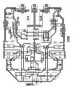
also to join the happy ksa cloners, i thought i should make one.
just finished revised pcb layout, based off ACD,s original.
should be easier to heatsink driver transistors.
Started revision to avoid cutting and jumping tracks for Q1, Q2
any feed back welcome before i etch the pcb,s
allan
ps R5 should be marked R145. i think.
just finished revised pcb layout, based off ACD,s original.
should be easier to heatsink driver transistors.
Started revision to avoid cutting and jumping tracks for Q1, Q2
any feed back welcome before i etch the pcb,s
allan
ps R5 should be marked R145. i think.
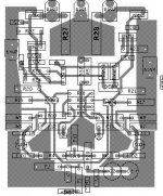
Attachments
still4given said:Yes, Merry Christmas!
Blessings, Terry
Merry christmas!
Man, wondering where the thread went for the last week...
Hi Awpagan,
why the big spacing between the small signal transistors? Much closer together and move r14 to r18 just a little to permit this. Can you turn the trs to face each other? then you can bond them together for thermal coupling.
Leave space around the plastic caps to allow the larger and much bigger pin pitch polypropylene if you think you may want to try these.
Where is your decoupling? Add bypass cap positions to all large uF caps. Leave a big space around the electrolytics to give flexibility of footprint.
The dual bias controller is a nice touch. Can you find the space for a little reed relay for remote switching (standby?) or summer/winter settings?
Can you move pads 1,2 &3 into the PCB? Then q9&10 can bolt onto a flat heatsink.
Depending on your chosen bias the VAS pair can run pretty warm. R22? & R23 are blocking effective sink space.
AndrewT
thanks for the reply
did look at turning the tansaround "thermally bonding". Havn't succeeded yet.
Was trying to keep signal length equal, for symmetry.
different caps
I thought of doing this (see attached) with earth and +/- .
"Can you move pads 1,2 &3 into the PCB? Then q9&10 can bolt onto a flat heatsink"
Flat heatsink, that was the idea.
pads were used till i made terminal block pinout.
If transistors on top with flat heatsink, the wires out have to run over the sink
Was thinking mount transistors from bottom to heatsink.
Relay? am thinking😀
All i was going for was a switch Dual bias
how about three position switch, high bias, warm bias for the sydney hot days and low bias for standby.
Seen any three position relays😀
allan
ps Q7, Q8 piece of flat alloy between them.
I'll move the pads inwards
Attachments
- Home
- Amplifiers
- Solid State
- Krell KSA 50 PCB