So I just got this Kicker 06 ZX1000.1 in as part of a partial trade towards other equipment. It’s “blown” is all I got, but power supply tested “good” via DMM on main terminals, charging caps, so I opened it up, safe to say I am the only one who’s ever opened this amp up in 16 years, all factory glue still intact.
I found the problem right away, you can see near recitifiers what looks to be “rods” near a hold down screw, found some stray wires near it and (yet again) looks to be the reason why this amp blew, making contact between those rods and the screw/heatsink. So far everything else tests good, removed all FETs and they all seem to be within spec. Inductor was bouncing around as well but still tests good at 200mH.
But I saw something I haven’t come across yet, so I asked other techs and was told it was prolly an engineer who did it, a “decoupler to reduce noise”? Per later board revision, components being unpopulated, and the fact all factory adhesives still instant, etc also pointing to a kicker engineer doing this.
My question is, is that little inductor marked 103.100v supposed to be connected from to pins on both of the BJTs as it looks? But it looks like it’s barely contacting one pin of the BJT the inductor is connected to ground. You can see in pic what I am talking about. Was the opposite inductor pin purposely attached to pins on both BJTs as it kinda looks or was it a quick job and the solder bled onto the other BJT as it also kinda looks like?
Any help or advise greatly appreciated, I’ll post more on physical board repair and other damage if I find any as I go through it. I only have JB weld on hand which it says it’s not electrically conductive and actually electrically insulative so going to use that. But ya this is a weird one for me, I only have maybe 10 boards Max under my belt and this is the first fine coming across an “engineering mod”.
Thx 🖖🏼
You can see the inductor in 1st pic, and the 2 pins it’s obviously supposed to contact, but is it supposed to contact the pin of the BJT the inductor is connected to via ground as well?
2nd picture is of damage, 3rd picture is the only one I could find that shows the area Undamaged, looks to me the rods just connect to that trace correct? There’s no trace on opposite side of board in that area.
Here is a better pic of exactly what I am asking about, circled in blue. Is that connection intentional or did the solder bleed over to that pin?
Desolder the cap. Those 2 legs are likely directly connected by the board. Attached is a photo I have of the same amp.
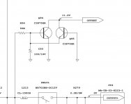
This may be the DC offset protection circuit. Attached is the DC offset protection from a different Kicker amp.
Testing the resistance across the power terminals doesn't indicate much other than there isn't a direct short (which would blow fuses). Many times, the FETs are all blown and all you'll see is the charging primary filter caps.
The added part marked 103 and 100 is a capacitor, not an inductor. 0.01uF @100v.
Rods?
Attachments
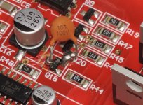
Ahh ok, so the it was intentional that one leg of the capacitor is connected to a leg of each 3875, it looks “barely” connected to one the legs, ty for clarifying with another pic.
The rod I’m referring to is the power/rail connected to the burnout on board.
Everything tested good on its own, I have repaired the burnt section of board by removing ALL carbonized/damaged board, filling with JB Weld (what I had on hand currently and is known as a good electrical insulator)
Continued to test board after installing each section of FETs, testing good all the way through, I now have board fully populated and fully functional.
I had a question on output banks, and how FETs were installed from Kicker factory, there’s 2 matching sets, assuming a matched pair for High and matched pair for Low, but when testing it looks like low gets one of each and high gets one of each, wouldn’t amp run better if both low side FETs matched and both High side FETs matched?
The circled and marked as is for banks in picture is correct right? Maybe the manufacturing dates are so close on FETs in didn’t matter when installing? I’d rather switch them up so each side has a matching pair.
Other then that I got lucky, just had to repair board and reconnect the rail to trace 🙂
I will be insulating by covering up the damaged board/exposed trace further but wanted to test first to make sure all is good beforehand.
Waves look good and everything nice and cool while running test tone with 12v/1.5a when idle
Waves look good and everything nice and cool while running test tone with 12v/1.5a when idle
Matching date codes (FETs from the same production batch) give the best chance of having FETs with very nearly identical properties and therefore likely to share the load evenly. For marginal designs, this gives the best reliability.
If the amp has survived this long with the FETs as they are, I'd leave them.
Those 'rods' are jumpers, hence the (assumed) Jxxx designation. They should not be confused with wire type shunt resistors.
I don't see anything that's circled.
If the amp has survived this long with the FETs as they are, I'd leave them.
Those 'rods' are jumpers, hence the (assumed) Jxxx designation. They should not be confused with wire type shunt resistors.
I don't see anything that's circled.
I just left them as is, but surprised they weren’t matched up per bank, maybe a tech made a mistake putting them in, etc, but ya they been going strong for this long right.
Also this is my first experience with jumpers, good to know more details on them, ty!
And the pic with the banks circled was the 2nd pic in post before last, you can scroll sideways to see all pics.
Also this is my first experience with jumpers, good to know more details on them, ty!
And the pic with the banks circled was the 2nd pic in post before last, you can scroll sideways to see all pics.
Post images on the forum, not on external servers.
I don't think manufacturers (or at least those who do the assembly) match FETs.
I don't think manufacturers (or at least those who do the assembly) match FETs.
- Home
- General Interest
- Car Audio
- Kicker 06 ZX1000.1 Rev1.4 (is this an Engineer mod?)