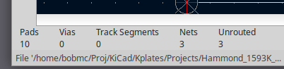
KiCad 6 "Update PCB From Schematic" produces PCB footprints nets, pads .. but no vias to connect them. I only wish to gerber a simple 2-layer PCB and have some confidence that a fab will accept it. Please tell me how I can complete update.
Attachments
Kicad schemtic does not know what layers you will use to make connections. When the schematic is brought into the PCB tool, the rats nest lines show what needs to be connected. Its up to you to do the routing and choose when to via up and down. In your case simple routing is all that is needed. Many videos on routing online.

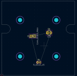
Many good tutorials online for how to use KiCad, most are not specific to V6 and the learning curve for any EDA tool is a bit steep at first. This menu is route tracks, if you hover over each icon it will tell you what it does. There is one for placing vias. I use them during routing traces to change layers, and I also use them to stitch together ground planes. This is a 4 layer board

Circled in blue is an example of two traces on different layers connected together by vias, make sure they have a net name assigned which will usually be the case if on a trace or plane. Circled in green are a couple of vias used for ground stitching. I don't normally use many through hole parts in my design, but this is an exception. 4 layers with 4 planes and traces routed on all layers.

Circled in blue is an example of two traces on different layers connected together by vias, make sure they have a net name assigned which will usually be the case if on a trace or plane. Circled in green are a couple of vias used for ground stitching. I don't normally use many through hole parts in my design, but this is an exception. 4 layers with 4 planes and traces routed on all layers.
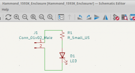
I was going to suggest a ground plane as well, but C1 and C2 should not be returned to it - use a net-tie to create a connection between J1-2 and the ground plane, the ground connections to C1 and C2 being returned directly to J1-2.
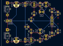
Capacitor charging currents do not flow through the ground plane, even ground planes have some resistance and large periodic currents flowing through the plane can make it noisy.
Schematic

PCB

Capacitor charging currents do not flow through the ground plane, even ground planes have some resistance and large periodic currents flowing through the plane can make it noisy.
Schematic
PCB
Last edited:
FWIW, there are some improvements to Net Ties coming in 7.0....
https://forum.kicad.info/t/post-v6-new-features-and-development-news/32633/61
https://forum.kicad.info/t/post-v6-new-features-and-development-news/32633/61
I would recommend audiotester.de for analog signal path measurements. I use REW for room and driver measurements, I have also used it to design analog parametric filters as well.
https://www.audiotester.de/
I am assume you are probably using LTSpice.
I've spent most of my career in analog/mixed signal and embedded hardware design.
https://www.audiotester.de/
I am assume you are probably using LTSpice.
I've spent most of my career in analog/mixed signal and embedded hardware design.
I am not a big fan of REW. It seems like designed by committee and everybody got their favourite feature. But REW works on Linux and other offerings do not. I think I would like audiotester if I had not abandoned Windows.I've spent most of my career in analog/mixed signal and embedded hardware design.
Most of my career was designing firmware for LIDAR. Mapping the ozone laser, creating digital maps with an airborne scanning laser, etc.
I understand about things not being supported in Linux, many years of fiddling around with WINE and loading win drivers in Linux with limited success. KiCad runs as well in Linux as windoz, and LTSpice runs well in Wine. I have so much stuff that needs windows I finally gave up on Linux about a decade ago. I also needed a good office program which basically meant Office. I have lots of devices that don't work in Linux unfortunately. My audio streaming hardware is all Linux based but it is basically plug and play, no editing config files etc in console.
- Home
- Design & Build
- Software Tools
- KiCad Routing Question