PMA said:Yes, their value (ratio) changes output DC offset.
it appears that selection of the R3 & R4 values comes first.EUVL said:
And of course, the Idss of the devices should be so chosen to give the same bias current with their corresponding source resistors. This means that their Idss should be different by a defined amount, depending on the value of the source resistors chosen.
Then select the Idss values to match the operating currents of the devices.
Finally trim either R3 or R4 to reduce DC offset to zero.
How do we select the ratio of R3:R4? Purely based on the published transconductance at our chosen operating currents?
Would that be the preferred procedure to get the best out of the pair of devices?
Or
Is there a better way to match non identical parameters?
And
The "ideal" approach is to measure the Id vs Vgs of each device. Then you fit the data using a, say 9th order polynomial. With the said equations, you can calculate the output linearity of the combined circuit including the source resistors. If you do this all by excel or mathcad, you can vary the resistor values until you get what optimisation you want (gain balance, minimum THD, or just H2, or .....).
The simpler, practical approach for gain balancing only :
I would not trust the datasheet, so I would at least measure transconductance at bias current first. Then you can decide on the source resistor values. Knowing that, the transconductance and bias current, you can then calculate required Idss. And the final fine trim by adjusting one of the source resistors.
Patrick
Well, now you know why I tend to use the matched pair N channel follower. For many years, even decades, I could easily get matched N channel fet pairs fairly cheaply. I first used the NPD5566 pairs for many years, I still have hundreds of them.
Parasound tended to use their own hand matched 170's or 2sk389's. These have somewhat higher transconductance and are somewhat better.
The automatic DC offset tracking allowed input and output connections without coupling caps.
It might be possible to slightly offset the Idss's of the N and P channel parts to get good DC performance with identical source resistors, or perhaps find a slightly different value for the N device and the P device, that 'might' give both low distortion and low offset. I have never taken it that far. This might be a good thing to simulate, IF the fet models are accurate enough.
All true.
My current favorite is the simplified Taylor current source as mentioned in my article (Fig. 3). It retains all the simplicity and low input capacitance of the all N-JFET follower, yet still allows push-pull operation and does provide better distortion cancellation.
It is particularly useful for high voltage / current applications, e.g. as a headphone amp using the LU1014 power N-JFET.
http://www.diyaudio.com/forums/showthread.php?postid=1593654#post1593654
http://www.diyaudio.com/forums/showthread.php?postid=1595627#post1595627
But we should really go back to John's circuits.
Apologies, John.
Patrick
The buffer below (has been posted by Edmond some 200 posts ago) with two curent sources would eliminate offset due to Idss differences, and the source resistance could be chosen accordingly to correct transconductance differences, without the need to find an Idss match.
Tino
Tino
Attachments
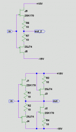
But that assumes that the K devices have the same Idss, and same for the J devices; right ?
Patrick
Patrick
Is a small offset any real issue? Servo would easily correct it. I would vote for simpler circuit, not to waste with CCSs.
Hi,
but it's not the error in Idss matching that is the problem.
It's the alleged difference in transconductance for the N & P types that causes the problem of unmatched currents in the operational condition.
The selection of differing Idss is a possible method of correcting for the transconductance difference.
source resistor adjustment
Can we make that connection between the circuits?
If there is improvement to be had for the simple two transistor buffer, then maybe the same method can be applied to the 4transistor input stage of the Blowtorch.EUVL said:
But we should really go back to John's circuits.
Apologies, John.
Can we make that connection between the circuits?
Hi, Mr. Curl,
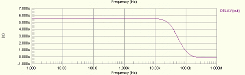
I wanted to ask you something. I've been trying to relate measurement with good sounding amps. I try to look at harmonics, it's difficult to relate. The FFT pattern seems have some relation with good sounding amps, but I cannot formulate this one.
Then I see a strong relation between good sounding amps with it's group delay and noise gain. These 2 can be generated in simulator (even better if we can measure it real time). Amps that have flat group delay and noise gain up until 20khz sounds nice. Amps that have bump or non-flat noise gain and group delay sounds not nice.
A good non-global feedback amps seems always have flat characteristic of these 2 factors. But global feedback amps also can be designed to have flat response of these 2 factors too.
Amps with same frequency response/flatness can have very different group delay and noise gain curve. I think this make different sound even the frequency response is about the same.
Can thiese 2 factors (noise gain and group delay) up to 20khz be a "clue" for a good sounding amps?
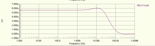
This group delay example sounds nice
I wanted to ask you something. I've been trying to relate measurement with good sounding amps. I try to look at harmonics, it's difficult to relate. The FFT pattern seems have some relation with good sounding amps, but I cannot formulate this one.
Then I see a strong relation between good sounding amps with it's group delay and noise gain. These 2 can be generated in simulator (even better if we can measure it real time). Amps that have flat group delay and noise gain up until 20khz sounds nice. Amps that have bump or non-flat noise gain and group delay sounds not nice.
A good non-global feedback amps seems always have flat characteristic of these 2 factors. But global feedback amps also can be designed to have flat response of these 2 factors too.
Amps with same frequency response/flatness can have very different group delay and noise gain curve. I think this make different sound even the frequency response is about the same.
Can thiese 2 factors (noise gain and group delay) up to 20khz be a "clue" for a good sounding amps?
This group delay example sounds nice
Attachments
EUVL said:Thank you Pavel for clarifying for us. You read John's mind much better than I can.
😉
It took me several years to understand, and now it is fine 😉
To clarify the present situation: I originally thought that PMA was addressing a problem that I was currently working on for the JC-1. I did not look at the schematic carefully enough and just saw two followers, rather than two DIFFERENT followers.
lumanauw,
Could you show us the schematic of the amplifier and show us the changes to improve the sound.
Jam
Could you show us the schematic of the amplifier and show us the changes to improve the sound.
Jam
How about degenerating the differential? I would like to see his solution and the root cause of the problem.
Jam
Jam
Hi, Jam,
I haven't drawn the schematic yet. The basic schematic that can give high enough and flat enough curve of noise gain and group delay until 20khz is folded cascode front end with heavy biased output stage.
Interesting thing is that the problematic curve shape is when it has bump somewhere. Non-global feedback amps can never have any bump in these 2 curves. Bumps only come when we apply global feedback (or active component inside feedback loop).
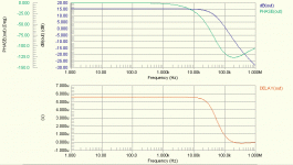
(green) is phase(deg), (red) is group delay (u_second)
I haven't drawn the schematic yet. The basic schematic that can give high enough and flat enough curve of noise gain and group delay until 20khz is folded cascode front end with heavy biased output stage.
Interesting thing is that the problematic curve shape is when it has bump somewhere. Non-global feedback amps can never have any bump in these 2 curves. Bumps only come when we apply global feedback (or active component inside feedback loop).
The curves I show you is not frequency response curve. They both have the same frequency response curve, the (blue) curve(dB).It looks like a stability issue.
(green) is phase(deg), (red) is group delay (u_second)
Attachments
- Status
- Not open for further replies.
- Home
- Amplifiers
- Solid State
- John Curl's Blowtorch preamplifier