I tried that long time ago... You could make it with mosfets, but I think that the thing with its sound signature is about loading (current modulation) of the phase splitter bjt, that you don't have with mosfets, except gate capacitances... I liked the bjt version better.
Could you give more details please?
Its good to see a departure from the old TO3 BJT formula. However, it does seem rather high dissipation for TO220 power transistors and suggests a hefty heatsink or two with best quality insulation material. Otherwise, its on my list for an original style matrix board build soon. I plan to use somewhat higher RDSS types IRF530 (not the N suffix variety). Any comment?Update
The asymmetry seems to be worse if the quiescent current is too high.
By reducing the current the simulation showed a better balance! (1 to 1.2A for 10W)...........Premature clipping (internally) not seen when power supply at 40V and driving 16W into 8 ohm load where Iq=1.5A.
Could you give more details please?
I already wrote what I think, what other details? It's a simple circuit and not that hard to adapt it for mosfets, if you are interested, you could try for your self and make your own conclusions.
...but I think that the thing with its sound signature is about loading (current modulation) of the phase splitter bjt...
Do you say overal sound signature mainly comes from the splitter? How about bjt splitter and MOSFET power stage, how it's going to sound in your opinion?
I originally proposed this as a 10W output, and the quiescent current for that is about 1A from 30V, so not so bad for a TO-220.
In general I prefer TO-3 for high powers; as they usually have better thermal characteristics, but recent TO-220's are improving. IR have largely done away with metal can FETs though.
Regarding the choice of device, I recommend higher current devices not for the current handling but the higher gain.
You guys might want to download the Nelson Pass PLH article done back in 2005 if I remember correctly where he shows 2 designs for a Mosfet based JLH amp.
I looked up Nelson's designs. As I thought, he only used a single input device (FET) and the output pair (the other design you mention is the same but with parallel outputs).
From my simulations the original configuration (bipolar input and driver) has lower distortion.
From my simulations the original configuration (bipolar input and driver) has lower distortion.
Attachments
OldDIY -
You've shown it's been done before. None quite match my design, but I'm sure if you keep digging you could well find it.
The circuit in your post #34 is closest, but I suggest a bootstrap is better unless you take a CCS transistor to a higher supply voltage.
The circuit in post #35 is not how I implemented driver transistors but does not meet my objective of keeping to 4 transistors.
The main advantage of the MOSFET output stage is the ability to work with lower load resistance. With the transition to class AB.
A higher supply voltage of 30-50V is required.
A higher supply voltage of 30-50V is required.
shaan
Some observations:
1. In the BJT version the bandwidth is ~2MHz, in the Lateral one it is ~5.5MHz(expecting oscillation and gate stoppers).
2. The rise time and fall time are respectively one sixth and half of that of the BJT version.
3. The BJT version had 0.2% distortion at 10VPP into 8ohm; the Lateral has 0.16%, with decreased higher order harmonics.
4. With +-20V supply, the BJT version has maximum voltage swing of 33V(+-16.5V), the Lateral has 30V(+-15V).
5. Clipping seems as good as the BJT one.
6. Maximum current output. This is where I am surprised. The circuit seems to be able to deliver current more than 2.5 times Iq. Initially I thought I made a mistake. But after many hours of experimenting no errors were found. I ran the sim at 1.6A of Iq, both the FETs can reach 4A when the load is down to 2ohm. I expected assymetrical clipping, as usual with the BJT version. At 1.6A Iq, the voltage at the gates of the FETs is ~2.7V.
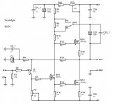
JLH 10 Watt class A amplifier

Some observations:
1. In the BJT version the bandwidth is ~2MHz, in the Lateral one it is ~5.5MHz(expecting oscillation and gate stoppers).
2. The rise time and fall time are respectively one sixth and half of that of the BJT version.
3. The BJT version had 0.2% distortion at 10VPP into 8ohm; the Lateral has 0.16%, with decreased higher order harmonics.
4. With +-20V supply, the BJT version has maximum voltage swing of 33V(+-16.5V), the Lateral has 30V(+-15V).
5. Clipping seems as good as the BJT one.
6. Maximum current output. This is where I am surprised. The circuit seems to be able to deliver current more than 2.5 times Iq. Initially I thought I made a mistake. But after many hours of experimenting no errors were found. I ran the sim at 1.6A of Iq, both the FETs can reach 4A when the load is down to 2ohm. I expected assymetrical clipping, as usual with the BJT version. At 1.6A Iq, the voltage at the gates of the FETs is ~2.7V.
JLH 10 Watt class A amplifier
- Home
- Amplifiers
- Solid State
- JLH10W- MOSFET output