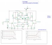
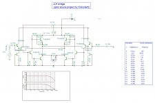
Why to bridge a JLH? Yes the output capacitors are eliminated . Yes the output power is doubled . But , these are nothing but gadgets of what is the outcome from bridging . The JLH is a single power supply classA amplifier . If it is bridged the power supply's current becomes exclusively DC , all AC components are canceled out mutually by the two branches . So what ? you may ask . In all amplifiers, the transient current to energize the speaker is relied upon discharging capacitor except in SE tube amplifiers where at half cycle the speaker is energized by the collapsing electromagnet of the output transformer that instantly spits it's electrons into the mouth of the speaker ,resulting higher definition , higher presence . With this amplifier the same phenomena ocurs but for full cycle, as the transient energizing current ,the amplifier has it already circulating in it's intestins .
It simply bursts it into the speaker instantly . Before I adventure with this project , I tried out this principle on a reduced scale by using two channel bridged amplifier IC the TDA1552Q with great success ,as it surpassed the definition of it's tutor , the great master , his majesty the 300B now "The obsolete" . See the Moon for six pence . In Bi-circleton , as the power supply is in series with the speaker I placed a mutual inductor . The inductor keeping the sum of the currents constant it also spits in both phases ,resulting expensive power supply . Whereas here ,an ordinary 24v/4a switching power supply will do the same job . By this the refrence amplifier that this amp should perform as good is no more the obsolete 300B although enhenced to 2A3C ,but the Bi-circleton . I created a new architecture or topology to make this amp not a pair of JLH bridged but a single JLH bridge amplifier . The feedback is an innovative differential one in comparing it with the input signal ,which also provides the required differential offset .
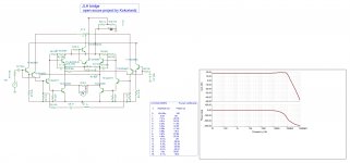
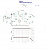
The quiescent operating point VCC/2 of the outputs is regulated by controlling the current of the current source of the differential input stage . Of course the bias current 1.5A on each branch is adjusted by the upper transistors base resistors . This is just a preliminary sketch I simulated it to see it functionality . The distortion 0.002% is mainly even order due to dissymetric feedback . Although it can be reduced to 0.0006% by dissymetric gain , I will first listen the sound as it is . The transfer function is of second order as the responce graph shows with fr about 10Mhz,on condition that the input source is low impedance . The output impedance shows 0.03ohms resistive up to 100khz . All these gives the amp it's chances to rival the open loop first order transfer function of the Bi-circleton. This project is to remain open source , This why I am posting it at preliminary stage to invite everyone for participation . Please give your opinion , critics, specially negative ones that might help see thing on different point of view .
Kokoriantz
the Moon for six pence bi-circleton
It simply bursts it into the speaker instantly . Before I adventure with this project , I tried out this principle on a reduced scale by using two channel bridged amplifier IC the TDA1552Q with great success ,as it surpassed the definition of it's tutor , the great master , his majesty the 300B now "The obsolete" . See the Moon for six pence . In Bi-circleton , as the power supply is in series with the speaker I placed a mutual inductor . The inductor keeping the sum of the currents constant it also spits in both phases ,resulting expensive power supply . Whereas here ,an ordinary 24v/4a switching power supply will do the same job . By this the refrence amplifier that this amp should perform as good is no more the obsolete 300B although enhenced to 2A3C ,but the Bi-circleton . I created a new architecture or topology to make this amp not a pair of JLH bridged but a single JLH bridge amplifier . The feedback is an innovative differential one in comparing it with the input signal ,which also provides the required differential offset .
The quiescent operating point VCC/2 of the outputs is regulated by controlling the current of the current source of the differential input stage . Of course the bias current 1.5A on each branch is adjusted by the upper transistors base resistors . This is just a preliminary sketch I simulated it to see it functionality . The distortion 0.002% is mainly even order due to dissymetric feedback . Although it can be reduced to 0.0006% by dissymetric gain , I will first listen the sound as it is . The transfer function is of second order as the responce graph shows with fr about 10Mhz,on condition that the input source is low impedance . The output impedance shows 0.03ohms resistive up to 100khz . All these gives the amp it's chances to rival the open loop first order transfer function of the Bi-circleton. This project is to remain open source , This why I am posting it at preliminary stage to invite everyone for participation . Please give your opinion , critics, specially negative ones that might help see thing on different point of view .
Kokoriantz
the Moon for six pence bi-circleton
Attachments
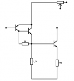
So the R13 is to tweak the distortion residue?
Why are you using BC338/328? 337/327 40 grade would be my first pick if I was designing something from scratch.
Another question - I see you are trying to eliminate as much caps from the circuit as possible - but it would seem that you could get an "soft/easy" response from the bias circuit if you replaced D1 with some suitable resistor and bypass the zener with a cap to make her silent.
The way you have it now you may be as well just amplifying zener noise and injecting it into both amp halves - and it may or may not cancel totally. Imho better kill it before it grows ... with a cheap cap.
Keep it simple!
d1 zener gone
Tina ti doesn't have grade 40 for these transistors . I do wonder if there are better Japanese ones .
R12 and R13 are feedback voltage dividers . If they are equal then the feedback is zero . If R13 is less than R12 the feedback becomes positive .
Tina ti doesn't have grade 40 for these transistors . I do wonder if there are better Japanese ones .
R12 and R13 are feedback voltage dividers . If they are equal then the feedback is zero . If R13 is less than R12 the feedback becomes positive .
Attachments
Ha ha ha I knew it you don't like capacitors (wrt bias circuit).
Ditto R12/13 - in other words, wrt what you mentioned in the OP, with R13 you effectivelly tweak the distortion from 0.002 to 0.0006. Cool ...
Ditto R12/13 - in other words, wrt what you mentioned in the OP, with R13 you effectivelly tweak the distortion from 0.002 to 0.0006. Cool ...
Really? I didn't know about that (the 3rd h inversion).
All I know is that P-type mos should have a bit lower noise than N-types...
But if you want to stick to the "proper" JLH theme, a BJT input would indeed be more PC. Also a BJT would make DC offset at output easier to handle.
What if you make a pnp darlington inputs (like a BC516 or so)? A darlington does some of the "fattening" as well but not as pleasant. Should be easier to get under control DC-wise, but would for sure require special compensation to get stable.
adjustments
The input transistors work at 400ua BDs 22ma . If I use Darlington the first transistor will work in nanoamp domain . Is it reasonable? The DMOS is used only for its non linear character. The input source still needs to be low .
Check the phase of the odd harmonics.
The input transistors work at 400ua BDs 22ma . If I use Darlington the first transistor will work in nanoamp domain . Is it reasonable? The DMOS is used only for its non linear character. The input source still needs to be low .
Check the phase of the odd harmonics.
Attachments
With darlington I meant to use a ready-made to92 device in the real build - but yep if you make a discrete version (2x pnp) for the sim the first one will be loaded pretty low. You can "cheat" some if you make the first pnp a something like 300-ish beta device, and the second one a 100-ish device (so cumulative around 30k beta, perhaps a little low for a store-bought darlington but close enough).
It seems that you made a topology that could be fitted with different type input pnp/p-types ... and almost auto-adjust (sans matching I guess). Way cool ...
WRT 3rd harm: is this a sim "bug" or you know that it indeed DOES that in real life? ...
It seems that you made a topology that could be fitted with different type input pnp/p-types ... and almost auto-adjust (sans matching I guess). Way cool ...
WRT 3rd harm: is this a sim "bug" or you know that it indeed DOES that in real life? ...

Did you think of effect that a "volume control" (a pot) would have on the performance?
The pot would insert a "variable source impedance" in the input leg of the circuit. This would in turn cause the amp compensation more difficult.
I had a very "not-good" experience with a cross-coupled opamp-based stereo-spread circuit, and this lates jlh schem of yours dosen't seem too far away from that topology.
Just a word of caution.
P.s.: It's just a gut feeling, but I think that your first topology has a beter "vibe" to it. But what do I know?
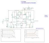
The JLH cannot have a volume . The source impedance must be very low ,unless as JLH suggests to use jfet source follower. This amp is eider driven directly by DAC or a preamplifier. The input impedance I raised to 10k with feedbacks 82k.It delivers 0.05%distortion at 18w to comply with the original at 9w.
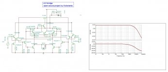
The precedent has reached it's maturity ,and it is time to switch to the next possibility. Only after having made a round trip of all ,than I decide which athlete has the best chance to compete against the Bi-Circleton .
The precedent has reached it's maturity ,and it is time to switch to the next possibility. Only after having made a round trip of all ,than I decide which athlete has the best chance to compete against the Bi-Circleton .

darlington inputs you said?
By adding emitter followers as LM3886 the performance got tripled . I really love this circuit . The four input transistors can be anything, I will place them on sockets and try out even jfets DMOS MOSFET . Have a look at the phases of the harmonics ,they are all in quadrant to the fundamental. I have never seen this .
By adding emitter followers as LM3886 the performance got tripled . I really love this circuit . The four input transistors can be anything, I will place them on sockets and try out even jfets DMOS MOSFET . Have a look at the phases of the harmonics ,they are all in quadrant to the fundamental. I have never seen this .
Attachments
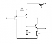
2sc5171
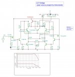
By replacing the bd139 with 2sc5171 the transfer function Bessel frequency nearly doubled 4.2Mhz . Unfortunately the simulated model unique I found on this website has a beta of 43 instead of 200 typical. So what concerns distortion I must see it on real model as 2sc5200 also needs to function at higher beta .
The input buffer has the function of providing the diff inputs low base impedance so that each can see the other as common base ,after which its pole becomes Ft ,the stage doesn't make part of the transfer function. Your proposition only higher the beta where I am decreasing it to adjust to Bessel.
I ordered on Aliexpress 10 pieces of fake 2sc5171 for 2$ I'll see what one gets . I think this topology has also reached it's maturity ,I will think for another .
Attachments
high frequency demper
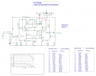
I tried to modify the JLH topology by using mosfet outputs diff. Input . I achieved Ultra Low Distortion Amplifier (ULDA) Ft about 10Mhz ,but unfortunately in bridge mode the result was disastrous. I'll post it after trying it out . I returned back to the precedent, but instead of decreasing the gain , I adapted a damper circuit to have perfect square wave . The result , distortion 0.0006%.
I tried to modify the JLH topology by using mosfet outputs diff. Input . I achieved Ultra Low Distortion Amplifier (ULDA) Ft about 10Mhz ,but unfortunately in bridge mode the result was disastrous. I'll post it after trying it out . I returned back to the precedent, but instead of decreasing the gain , I adapted a damper circuit to have perfect square wave . The result , distortion 0.0006%.
Attachments
- Status
- Not open for further replies.
- Home
- Amplifiers
- Solid State
- JLH bridge