Hello,
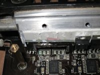
I am working on repairing a JL HD750/1 that had 2 of the 4 output MOSFET shorted (ordered 4 FDP2552 replacements yesterday). When I removed the heat sink clamp from the output MOSFETS there is a secondary PCB that is perpendicular to the main PCB. That daughter PCB (labeled thermistor board) connects to R554 terminals of the main PCB, and surrounds two of the output MOSFETS and has a few SMD components on it. One of the components near the MOSFET drain flanges has some thermal gap pad covering it, but two of the components (labeled capacitors) did not have any pad covering them.
It looks like the terminals of the capacitors were free to short out to the drain flange of the MOSFET. I can see where the ends of the components left marks on the flange in the attached image.
Am I missing some isolation pad on these two components, or is this normal? If it is normal, what is the function/goal of these two capacitors against the drain flange?

Daughter PCB, thermal gap pad in the middle covers one SMD component. The two outer SMD capacitors are not covered, and press against the the drain flange of the MOSFET, effectively shorting the terminals of the capacitor together.

Opposite side of the daughter PCB.

Marks on the removed MOSFETS.
I am working on repairing a JL HD750/1 that had 2 of the 4 output MOSFET shorted (ordered 4 FDP2552 replacements yesterday). When I removed the heat sink clamp from the output MOSFETS there is a secondary PCB that is perpendicular to the main PCB. That daughter PCB (labeled thermistor board) connects to R554 terminals of the main PCB, and surrounds two of the output MOSFETS and has a few SMD components on it. One of the components near the MOSFET drain flanges has some thermal gap pad covering it, but two of the components (labeled capacitors) did not have any pad covering them.
It looks like the terminals of the capacitors were free to short out to the drain flange of the MOSFET. I can see where the ends of the components left marks on the flange in the attached image.
Am I missing some isolation pad on these two components, or is this normal? If it is normal, what is the function/goal of these two capacitors against the drain flange?
Daughter PCB, thermal gap pad in the middle covers one SMD component. The two outer SMD capacitors are not covered, and press against the the drain flange of the MOSFET, effectively shorting the terminals of the capacitor together.
Opposite side of the daughter PCB.
Marks on the removed MOSFETS.
Attachments
The resolution is not good enough to see much but are C2 and C3 (?) on the small board connected to any traces on that board?
I probed around with my DMM set to Ohms and it does not appear that they are connected to either terminal.
You think they are just spacers or that they are using them to transfer heat?
You think they are just spacers or that they are using them to transfer heat?
I was thinking spacers. I can't see any detail for the thermistor (location, shape, contact surface...).
Okay, spacers sound reasonable. I check the other HD750/1 I have and it is the same, so it seems unlikely that an isolation pad is missing.
- Home
- General Interest
- Car Audio
- JL HD750/1 output R554 question