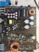
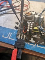
So, back to this amp. Somebody tried already bad repair job... So, if i mount the ps fets, they open directly if i connect b+ and - without remote. Removed some diodes, now its ok, but i have no amplitude. Somehow there is all the time something like a small sine wave between gate and source, but also on all other transistors. So which part is for the power supply modulation?
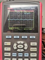
Quote: The sinewave is from our power net...Somehow it was affecting my measurments.
Quote: The sinewave is from our power net...Somehow it was affecting my measurments.
Attachments
Last edited:
I have a 3808A Low power current mode push pull pwm controller, beside is a l339 Quad comparator. Damaged is a rectifier Sf1606G . One leg is shorted to center. The other diodes, i dont know the funktion, but the diodes are ok, but if i measure with diode test the solder place, one direction shows short, if i change the measure tips direction, then its ok.
The controller is ok, and shows a good amplitude... But i cant find, where the signal goes..
Found now, that the signal goes into a TC4427E, driver chip. Input is ok, output is floating.
The controller is ok, and shows a good amplitude... But i cant find, where the signal goes..
Found now, that the signal goes into a TC4427E, driver chip. Input is ok, output is floating.
Last edited:
These are rough notes from a 600/4. I have no idea if they're even remotely close to what you have.
Remote turns on Q505 and the collector remains low as long as remote is applied.
Q504 pulses on but as soon as D508 reaches breakdown voltage, it's driven off and remains held off as long as D508 is above threshold voltage.
Q503 controls the low-voltage/driver supply. It allows the supply to power up when Q505 pulls to ground (when remote voltage is present). It stops conducting when Q505 is switched on. This allows it's drain to go high and allows the driver IC to produce output pulses. D513 allows it to be switched off immediately (gate pulled towards ground). This allows the LV supply to immediately switch on.
When remote is voltage is removed, the collector of Q505 immediately goes high but the voltage on the gate of Q503 doesn't immediately go high enough to turn Q503 on. The voltage is delayed because the cap C541 is slowly charged by the 10M resistor two places below R501. This gives the LV supply a 15 second delay turning off (like other JL amps).
When Q503 is not conducting (remote voltage present or turn-off delay), it's drain is at approximately 2.5v which allows the comp pin of U503 to be the same and the IC produces output. So, Q503, immediatly switched of with remote and during the off delay.
Q500 controls the main supply that produces rail voltage. When Q505 switches on (remote on), Q500 switches off and allows its collector to go high (2-3v). This allows the main supply to power up. Q500 switches on and off with remote with no delay.
Received the new parts, and still working on the remote. I cant find, from where the UCC3808 get his voltage. Found the transistors and diodes, that you mentioned. Found also, that the voltage on one transistor swing from 0 to 1.2 V ... But no direct connetion to the pwm driver..
No, but anyway, something is pulling the Remote +12V down...so i think there are more issues.
Not sure it's relevant to your model but the older slash amplifiers required this daughter board to be in circuit for the power supply to operate.
yes, seems xyou are right. The led is flashing green red now.
But my ic´s are wrong. At ic 504 i expected a pwm driver, but i have at pin 7 11VDC without the three ic´s inside. According datasheet, this should be a output.. So, if somebody know the correct markings or part numbers, it would be very helpful.
But my ic´s are wrong. At ic 504 i expected a pwm driver, but i have at pin 7 11VDC without the three ic´s inside. According datasheet, this should be a output.. So, if somebody know the correct markings or part numbers, it would be very helpful.
I don't have any photos of this amplifer. But this is from another thread. Zoom in on the photo: https://www.diyaudio.com/forums/att...ion-help-15503275746864724323072917756905-jpg
- Home
- General Interest
- Car Audio
- JL HD750/1 burned Power supply