I “drilled” out the broken via, just large enough to fit 3 hair thin copper wires, twisted, through the PCB, soldering each end to the trace the Via was supposed to connect. I made sure no other connections were made and everything is clean clean on point. Putting everything back together now, I’ll report back once I have.
Attachments
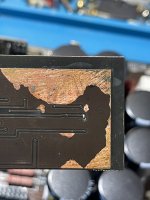
I use a #80 drill bit to drill through whatever is in the via and a single strand of wire (just smaller than the drill bit) to re-establish the connections.
Last edited:
Ya the copper wire I chose was like hair thin, figured 3 twisted up was good 🙂 def gona keep my modeling drills out, didn’t even consider this to be a thing, learning something new every repair 🙂
thx again Perry, really appreciate it bro 🙂
fully populated running smooth 🦾🤓🔊
thx again Perry, really appreciate it bro 🙂
fully populated running smooth 🦾🤓🔊
Attachments
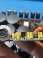
JL 1000/1 was running good right, so I decided to use it this morning to test a sub I just rebuilt since it’s already on my test bench ...powers on proper Green but no output ...so I throw it on the work bench, pull a clamp cover off a set of power & output FETs, output has switching, but 1 of the Power FETs displays this, and the other flatline ...I’m in the process of pulling it from the case HS now.
What would cause this wave? Related to the via break in anyway? I doubt it but wanted to ask, about to check everything and see what is/isn’t switching, etc.
I do know these amps will still “run” even when there’s problems, ******** tanks man lol 😅
pic is of Q813 tab, Q812 isn’t showing any switching on tab
Attachments
Ok, looks like all even Q power supply FETs are push and the odd Q power supply FETs are pull (or vice versa) hence square wave on the tab of odd Q FETs and wave on 3rd leg of even Q FETs? Maybe I’m overthinking it but I thought I would see waves on both Tabs of the Push & Pull FETs.
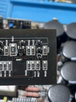
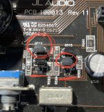
I replaced the 2 circled pre-drivers 1st thing when recieving amp, ran power through amp, then realized I never checked the 2 underlined BJTs, which were bad, so I replaced those as well much later after some power cycles, I’m thinking those bad underlined BJTs did enough damage to the new replaced circled pre-drivers to seal their fate ...both circled pre/drivers are bad again but underlined BJTs are still good, replacing the pre-drivers again now 😅
Attachments
The power supply is a full-bridge, not the standard push-pull.
Did you do any work on the high-side driver boards?
Did you do any work on the high-side driver boards?
Ahh ok, ty for clarifying 🙂
New pre-drivers I just installed are dead as well, must’ve been killed on power up, soon as I booted up I probed Tab of odd Labeled Q PS FETs and no change, I think the underlined BJTs under them are dead as well even tho they don’t test bad? Both sets were bad originally.
And no, no work don’t anything other then this buffer/pre-driver area (last pic posted, those 4 components circled/underlined) and the corrosion/via break on daughterboard.
Also, just a side note I wanted to mention, I thought some JCJ 111 were bad, but the same 2 legs, on 3-4 diff areas of board, all test about 24 Ω, which ended up being the board pads testing like that not the transistor itself, so I figured since they all same Ω range it must be a design thing? Just wanted to bring it up, just in case.
mans to be clear Q512 and Q517 are the transistors that keep dying
mans to be clear Q512 and Q517 are the transistors that keep dying
Attachments
Confirm that those are the drivers for the output stage.
Why do you think the transistors are defective, even when checking to be OK?
Are you sure that the J111 transistors are defective? They're jfets and don't read like other transistors.
Why do you think the transistors are defective, even when checking to be OK?
Are you sure that the J111 transistors are defective? They're jfets and don't read like other transistors.
So I’m an idiot Perry, I apologize. The transistors at Q512 & Q517 are in fact good, even the ones I just pulled prior are still good, the pads are connected via a teacd. This is not the problem area, confirmed by you confirming this are pertains to the output stage 😅
The reason I thought all of the J111’s were bad is because 2 legs read as 24-ish Ω, which is usually close to a dead short, but all of the J111 pads test at that ohmage, not the actual JFETs themselves. I just wanted to bring it up, just in case, but I’m sure the board is designed that way since all of them test that way.
I am reinstalling the transistors now, so as of right now board is 100% populated as it was when working last night, but is not working, that funky square wave still on the PS FETs
I don't see a problem with the PS. That type of supply has the drain of half of the transistors connected to the B+ supply and will always have straight DC on them.
The jfets will/should read low resistance D-S out of the circuit.
Pulse the remote for a second to start the low-voltage supply. When the LV supply is running, do you see a drive signal on the output transistors?
The jfets will/should read low resistance D-S out of the circuit.
Pulse the remote for a second to start the low-voltage supply. When the LV supply is running, do you see a drive signal on the output transistors?
Ok, ty for clarifying, I think this is the only full bridge I’ve worked on so far, plus it’s a JL Audio 😅
JFETs do, ty
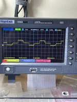
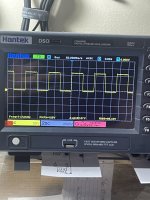
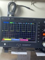
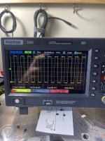
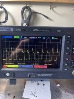
yesterday, when amp was fully working the PS drive looked like 1st pic, classic square wave, 2nd pic is output switching (forgot to adjust scope, but it was still clean) now that amp is not working the 3rd pic is what switching looks like on PS (funky stepped square wave) and 4th pic is output as of right now. I do not have a pic of previous rectifier waves but the waves on the out rectifier closest to PS FETs now are in 5th pic, never seen them that way before. Isn’t that huge spike due to ringing, could that be what’s messing up the PS drive? Or is the funky PS drive wave messing the rectifier waves up.
pics:
1,2
3,4
5
mill try to pulse so Lv supply kicks on and get a pic of output drive wave. How do I know if LV supply is on again? When I pulse the remote the amp just seems to turn on as normal once rail voltage is reached, my Power Supply can start and run it, idles at 3a
JFETs do, ty
yesterday, when amp was fully working the PS drive looked like 1st pic, classic square wave, 2nd pic is output switching (forgot to adjust scope, but it was still clean) now that amp is not working the 3rd pic is what switching looks like on PS (funky stepped square wave) and 4th pic is output as of right now. I do not have a pic of previous rectifier waves but the waves on the out rectifier closest to PS FETs now are in 5th pic, never seen them that way before. Isn’t that huge spike due to ringing, could that be what’s messing up the PS drive? Or is the funky PS drive wave messing the rectifier waves up.
pics:
1,2
3,4
5
mill try to pulse so Lv supply kicks on and get a pic of output drive wave. How do I know if LV supply is on again? When I pulse the remote the amp just seems to turn on as normal once rail voltage is reached, my Power Supply can start and run it, idles at 3a
Attachments
-
 FF942187-EE1A-455B-9FE1-4B86316284D2.jpeg454.8 KB · Views: 64
 -
 18627EC6-5A24-4A28-89FC-CD96DBFDA370.jpeg460.8 KB · Views: 59
 -
 E0CB245F-4E66-46F5-80C4-2CC1102A03A4.jpeg482.5 KB · Views: 45
 -
 E970DDD7-0248-4E8B-87F1-A30916BF3496.jpeg500.2 KB · Views: 48
 -
 B3BC7F48-3347-4E48-997F-B9F235F4BAFF.jpeg451.7 KB · Views: 56
Did you read the JL 1000 page of the tutorial?
This is a regulated power supply. The waveforms will look different before and after the target rail voltage has been reached. Vary the DC voltage feeding the amp and you should see the waveforms change.
This is a regulated power supply. The waveforms will look different before and after the target rail voltage has been reached. Vary the DC voltage feeding the amp and you should see the waveforms change.
No, I don’t think I knew one was there but I may have forgotten, going to read it now!
ok. Yes I see a drive wave on Output growing during pulsing, until either low voltage LED kicks on and amp shuts down or amp eventually reaches rail and boots up fully.
Off to read the JL 1000/1 tutorial to see if I can find a reason for these funky PS waves and no output, everything I repaired has stayed repaired so it’s def something new 🥴 lol
- Home
- General Interest
- Car Audio
- JL Audio Slash 1000/1 Rev.11 *Low Voltage*