Just a quick question regarding the loss in signal amplitude from gate to source in JFETs.
The output impedance out of a JFET follower is 1/Gm is it not? (Or is it 'Yfs' in JFETs and not 'Gm'?) What is the difference in 'forward transfer admittance (Yfs)' and transconductance (Gm)?
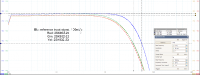
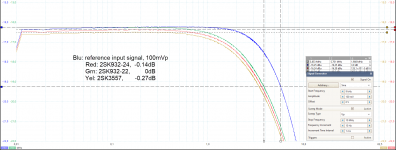
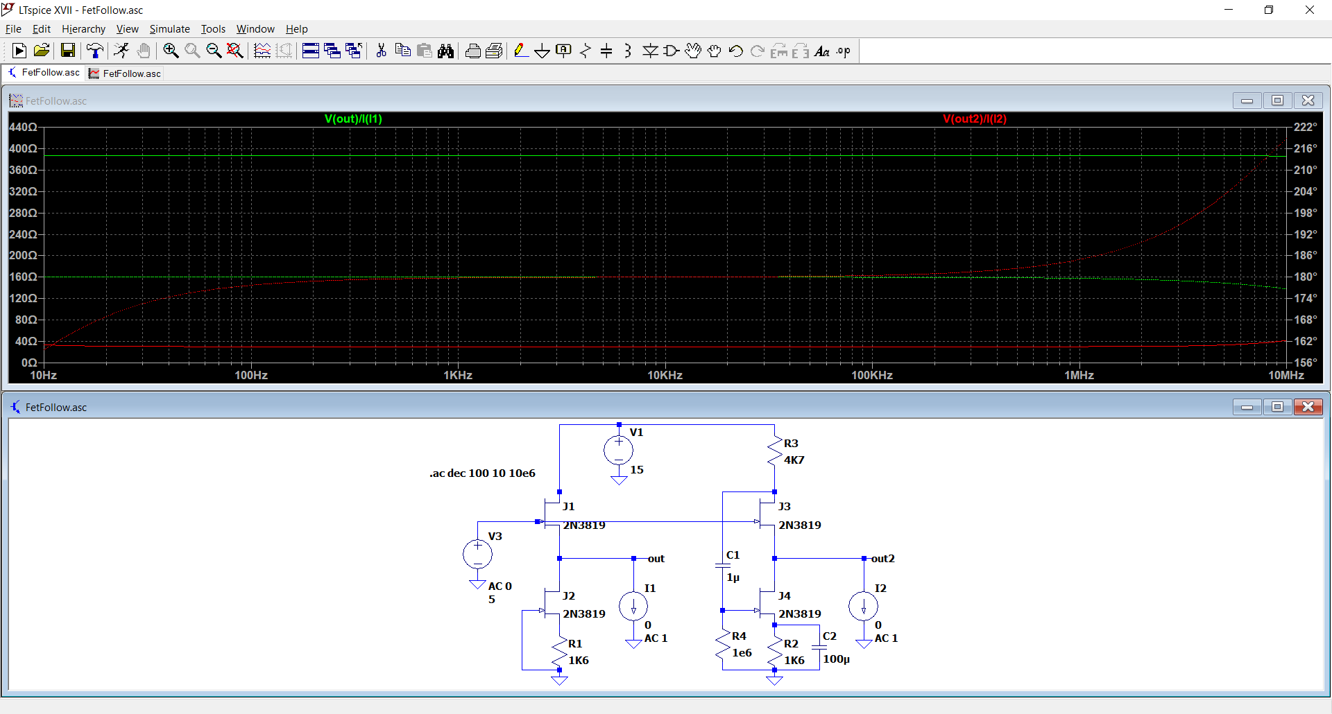
I have a buffer ckt using a JFET as follower, and in the bottom (JFET source) there is a CCS made up of another JFET, a 2SK3557 biased at ca 1mA. The load is a 10kohm resistor (the next stage opamp).
Using a CCS for biasing, there should be very little loss in amplitude, when the load the JFET buffer is driving is relatively high in impedance.
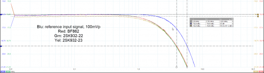
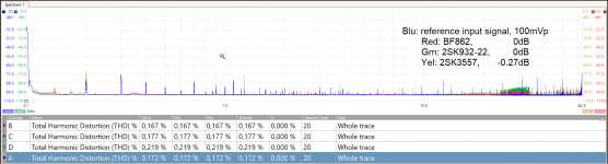
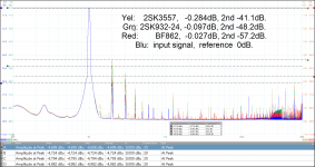
I have tested this using BF862, 2SK932, and 2SK3557. The BF862 and 2SK932-22 have no loss, the 2SK3557 has ca -0.3dB loss.
The 2SK932 come in sorted by IDSS in 3 grades, where the -22 has the lowest IDSS and the -24 has the highest. The -22 has no loss like the BF862, but the -23 and -24 have little under 0.2dB loss.
I assumed the highest IDSS version would have the best, or strongest, drive, and give the least amount of loss, but it is the other way, the lowest IDSS version gives the least loss. Is this always the case? Should I select low IDSS JFETs for source follower duties?
I included some distortion measurements and the 2SK3557 is not very linear as a follower, at least at this low current. The BF862 has slightly better figures than teh reference input signal, probably because it's linearity is slightly opposite the testsignal or something. Or it is just so low that the scope cant measure accurately.
I am a little surprised the JFETs loss when used with a CCS and driving 10kohm.
Anyways, I just thought this slightly interesting and perhaps some one else is experimenting with these JFETs.
The output impedance out of a JFET follower is 1/Gm is it not? (Or is it 'Yfs' in JFETs and not 'Gm'?) What is the difference in 'forward transfer admittance (Yfs)' and transconductance (Gm)?
I have a buffer ckt using a JFET as follower, and in the bottom (JFET source) there is a CCS made up of another JFET, a 2SK3557 biased at ca 1mA. The load is a 10kohm resistor (the next stage opamp).
Using a CCS for biasing, there should be very little loss in amplitude, when the load the JFET buffer is driving is relatively high in impedance.
I have tested this using BF862, 2SK932, and 2SK3557. The BF862 and 2SK932-22 have no loss, the 2SK3557 has ca -0.3dB loss.
The 2SK932 come in sorted by IDSS in 3 grades, where the -22 has the lowest IDSS and the -24 has the highest. The -22 has no loss like the BF862, but the -23 and -24 have little under 0.2dB loss.
I assumed the highest IDSS version would have the best, or strongest, drive, and give the least amount of loss, but it is the other way, the lowest IDSS version gives the least loss. Is this always the case? Should I select low IDSS JFETs for source follower duties?
I included some distortion measurements and the 2SK3557 is not very linear as a follower, at least at this low current. The BF862 has slightly better figures than teh reference input signal, probably because it's linearity is slightly opposite the testsignal or something. Or it is just so low that the scope cant measure accurately.
I am a little surprised the JFETs loss when used with a CCS and driving 10kohm.
Anyways, I just thought this slightly interesting and perhaps some one else is experimenting with these JFETs.
Attachments
Just a quick question regarding the loss in signal amplitude from gate to source in JFETs.
The output impedance out of a JFET follower is 1/Gm is it not? (Or is it 'Yfs' in JFETs and not 'Gm'?) What is the difference in 'forward transfer admittance (Yfs)' and transconductance (Gm)?
The transconductance is the real part (part without phase shift) of the transadmittance. For low frequencies (say < 30 MHz) they are essentially the same.
The FET also has a conductance between drain and source (common-source output conductance gos) that effectively loads the source follower. It's the derivative of the drain current to the drain-source voltage in the ID versus VDS graph. Maybe that causes your small gain loss.
Isn't 1mA of bias much too low?
Hi. Yes for audio it probably is, but the goal is very low current draw from a small battery. I can try same at higher, say 10mA just for interest of comparing the devices and the loss (which should be less since Gm increases).
The transconductance is the real part (part without phase shift) of the transadmittance. For low frequencies (say < 30 MHz) they are essentially the same.
The FET also has a conductance between drain and source (common-source output conductance gos) that effectively loads the source follower. It's the derivative of the drain current to the drain-source voltage in the ID versus VDS graph. Maybe that causes your small gain loss.
Thanks, I kinda thought Gm and Yfs is the same...
You worry about 0.3dB loss?the 2SK3557 has ca -0.3dB loss.
In a low current simple follower stage?
I´m amazed at the excellent performance!!!
Ha - jepp I guess 0.3dB is asinine nerdy. Mostly I was just checking the three grades of 2SK932, which are selected in 3 grades of IDSS. When I found the lowest IDSS version drove the load with out any loss, I started looking into it. This surprised me because I thought the higher IDSS indicates higher Gm, but thinking harder I see the Gm is very similar, it is the IDSS that varies drastically in devices. (Gm in JFETs vary only by SQRT of Id so I guess that makes sense). This is actually what prompted my thread, - which IDSS to chose from when selecting a JFET for buffer service. Then I noted the higher distortion in the 2SK3557 and desided to compare to BF862 and 2SK932. I figure I am not the only one having to replace the BF862, so perhaps interesting for others to see. Granted this is at Vdd of only 3.3V and Id of 1mA, so as you say pretty good actually. But I cannot get words right, I am very confused in general and cant seem to write the simplest questions.
To increase the performance and make the output stiffer, you could wrap a Taylor or White-style circuit around the FET.
It might be a little more complicated than a simple CCS sink, but if you are looking for top performance, it is a worthwhile option
It might be a little more complicated than a simple CCS sink, but if you are looking for top performance, it is a worthwhile option
Ha - jepp I guess 0.3dB is asinine nerdy. Mostly I was just checking the three grades of 2SK932, which are selected in 3 grades of IDSS. When I found the lowest IDSS version drove the load with out any loss, I started looking into it. This surprised me because I thought the higher IDSS indicates higher Gm, but thinking harder I see the Gm is very similar, it is the IDSS that varies drastically in devices. (Gm in JFETs vary only by SQRT of Id so I guess that makes sense).
Usually the higher IDSS grade FETs of the same type have a higher IDSS, but also a higher pinch-off voltage (higher absolute value, that is).
I'm about to speculate now, so I hope someone who knows more about JFET device physics corrects me if it's nonsense:
I guess they have thicker channels that conduct more current at VGS = 0, but also need a more negative VGS for the whole channel to get depleted. In the end it's like the whole ID versus VGS curve shifts to the left. With a fixed source current (constant current source biasing), you end up at essentially the same point of the curve, just shifted to the left along the VGS axis.
You meant lower IDSS, higher transconduntance?
I think the last two sentences of what I wrote in post #9 are nonsense anyway, as is post #11. I implicitly assumed that the depletion layer's thickness has a straight line dependence on -VGS, but in fact it is closer to a square root.
Last edited:
Here is a comparison between a regular follower, and the same with the White components added:
The output impedance is improved by one order of magnitude.
The penalty is a severely degraded PSRR.
A Taylor circuit eliminates that issue.
The output impedance is improved by one order of magnitude.
The penalty is a severely degraded PSRR.
A Taylor circuit eliminates that issue.
Attachments
....the lowest IDSS version drove the load with out any loss, I started looking into it. This surprised me because I thought the higher IDSS indicates higher Gm....
It IS surprising.
What is your in-circuit Vgs? I assume all three devices are worked at nearly the same current? Then the low Idss part may be near zero Vgs, the high-Idss part may have a large Vgs; and that large Vgs may be more "flexible" with more signal "loss".
Obviously devices of the same geometry have a relationship between Vp and Idss so "something" will trend the same way, but too much for my brain.
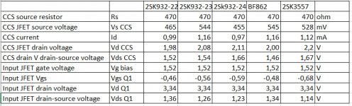
The Vgs is ca -0.5V for all of them. Here's measured values:
Attachments
Last edited:
I think the last two sentences of what I wrote in post #9 are nonsense anyway, as is post #11. I implicitly assumed that the depletion layer's thickness has a straight line dependence on -VGS, but in fact it is closer to a square root.
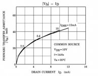
No, a given geometry JFET has very little variation in gm vs Idss at a constant current, this is obvious just by looking at a data sheet graph. How many times do I have to post this graph (2SK170)?
Attachments
Last edited:
Yes, find Shockley's original JFET analysis with all the equations you will see the Vp^^2/Idss relationship with very weak variation due to other parameters. I only have an ancient xerox of it and can't find it on the web right now, but yes you were right.
- Home
- Design & Build
- Parts
- JFET source follower drive strength