My Take on making a folded cascode op amp.
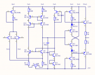
Figure 1 shows the concept I have followed. It is from the AD8021 datasheet.
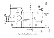
Figure 2 is my op amp.
The several JFET CCS resistors needs to be adjusted to suitable currents.
I have put a target of 2mA in all stages.
The output is a buffer using two schottky diodes. They drop like 0.3V at 2mA.
That 0.3V is put across each resistor in the output.
The amplifier will work in Class A downto like 1k loads.
100pF compensation cap is probably overcompensation.
But just want the amplifier to be stable.
Power supply can be upto +/-25V.
The chosen JFETS are for max 50V.
Figure 1 shows the concept I have followed. It is from the AD8021 datasheet.
Figure 2 is my op amp.
The several JFET CCS resistors needs to be adjusted to suitable currents.
I have put a target of 2mA in all stages.
The output is a buffer using two schottky diodes. They drop like 0.3V at 2mA.
That 0.3V is put across each resistor in the output.
The amplifier will work in Class A downto like 1k loads.
100pF compensation cap is probably overcompensation.
But just want the amplifier to be stable.
Power supply can be upto +/-25V.
The chosen JFETS are for max 50V.
Attachments
-For optimal power supply rejection, you could connect the compensation capacitor to ground rather than to -25 V.
-Don't use a carbon trimpot for P1, as their wipers slowly become anodized when there is current flowing out of the wiper (into the wiper is OK).
-I think your circuit is free from undesired bias points due to polarity reversal issues, even when used as a voltage follower. The current source of the first stage always has some voltage, even when both inputs are close to +25 V, and you have to drive the inputs all the way to the negative rail to get the drain-gate diodes of the input FETs into forward bias - which normally won't happen due to the voltage drop across the output stage.
Summarizing: looks good!
By the way, JFET gate leakage current tends to increase at high VDS and high ID. That has something to do with impact ionization, but I don't know the details.
JFET gate leakage current tends to increase at high VDS and high ID.
On P-JFETs such as the 2SJ103s that lineup has chosen, the IGSX - VDS increase rate is slower than with N-JFETs, but the effect is still present.
Last edited:
That is true. Compensation cap.-For optimal power supply rejection, you could connect the compensation capacitor to ground rather than to -25 V.
-Don't use a carbon trimpot for P1, as their wipers slowly become anodized when there is current flowing out of the wiper (into the wiper is OK).
Summarizing: looks good!
But most op amps do not have a ground connection pin.
So I chose the second best option.
Of course I could make such a 'pin'.
For more optimal performance I could select a 22pF/47pF instead of the 100pF.
Probably can get away with that.
I fancy Bourns conductive plastic potentiometers.
It feels better than having carbon.
Hi lineup,
May I suggest to move P1 to Q4/Q5 emitters (and adjust R2/R3 value accordingly (something like 150R for resistor and 1-5k for P1)...
...or move P1 to Q6/Q7 emitters (and adjust value for P1 accordingly)
Regarding compensation you could connect C1 to Q2 gate (value should be like 10pf)
May I suggest to move P1 to Q4/Q5 emitters (and adjust R2/R3 value accordingly (something like 150R for resistor and 1-5k for P1)...
...or move P1 to Q6/Q7 emitters (and adjust value for P1 accordingly)
Regarding compensation you could connect C1 to Q2 gate (value should be like 10pf)
Last edited:
- Status
- Not open for further replies.