I am planning on swapping the BJT's in my differential pair input stage on my amplifier design with JFET's, mainly to effectively eliminate base current, and found the LSK170 on the DIYaudioStore
Linear Systems LSK170 Ultra Low Noise Single N-Channel JFET (8 Pieces) – diyAudio Store (BETA)
But I also found the PN4393 on digikey for much cheaper
PN4393 TRA Central Semiconductor Corp | Discrete Semiconductor Products | DigiKey
What are the advantages of the LSK170 over the PN4393? It seems noise, but is that all? And how noisy would the PN4393 be?
Also how do I go about changing the biasing for the JFET's? My diff. pair has a current mirror and current sink set to 3.5mA total, but it seems the Idss is greater than that even with the grade A LSK170 and I'm assuming this would mean a negative gate to source voltage. Is this a problem?
Thanks!
Try matched monolithic n channel JFET pair LSK389.
http://www.linearsystems.com/assets/media/file/datasheets/LSK389.pdf
http://www.linearsystems.com/assets/media/file/datasheets/LSK389.pdf
hi,
just checking ... it wasn't clear from your comments so i'll ask ...
you do know just dropping in jfets to replace bjts in a straight swap is not likely to be successful, right?
mlloyd1
just checking ... it wasn't clear from your comments so i'll ask ...
you do know just dropping in jfets to replace bjts in a straight swap is not likely to be successful, right?
mlloyd1
I am planning on swapping the BJT's in my differential pair input stage on my amplifier design with JFET's ...
You can run the jFETpair at 3.5mA.
Each jFET should pass exactly half that bias current.
The jFETs can be biased to pass any amount of current upto Idss and a tiny bit more.
It is usual to bias jFETs in an LTP @ between 50% and 90% of Idss.
They work well in this range.
You will find some Builders using 10mA Idss devices and operates them at <<1mA of bias.
I can't understand why that should be done.
If you choose not to change the 3.5mA bias current, then you can use A grade lsk170.
The lowest A grade is 2.6mA for Idss. Running at 1.75mA is equivalent to biasing @ 67%
Look at the datasheet. You will see that the gm for a 2.6mA device is identical to a 5mA device and to a 12mA device.
There is no advantage to using a high Idss device when the bias is set very low.
The same applies to other jFET types.
Bias at 50% to 90% and limit dissipation by limiting Vds. A jFET cascode is ideal for this.
There is likely to be some performance benefit to increasing the input LTP bias to well above 3.5mA. Think about 5mA, or even 10mA.
This would require a slightly higher Idss device and a check for max dissipation.
Last edited:
Replacing the BJT to JFET can improve dealing with the Input Bias Current, but degrade the Input Offset Voltage due to variation of the JFET Ugs, and generally worsen the situation. In addition, it may decrease the gain input stage for voltage and depth of feedback that will increase the distortion of the entire amplifier. You've got to be careful and know what you're doing.
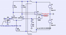
For semi-automatic selection of matched pairs of JFET and BJT. 🙂
The idea is that the OpAmp drove the J2 and balanced currents J1 and J2. In place of the J1 and J2 through connector placed a pair of JFET or BJT, and the output OpAmp to measure the voltage of the error and pick up a pair of JFET or BJT at the lower value.
For the selection of the BJT R2 = R3.
You can choose OpAmp any cheap device.
Attachments
Last edited:
- Status
- Not open for further replies.
- Home
- Amplifiers
- Solid State
- JFET differential pair trans. choice