Hello RCruz,
For the "short gate" (??) JFETs like 2SK170 it should be better to operate them at or close to Idss as the transfer curve becomes more linear so THD should go down with higher current. I think John Curl has stated this before. For the "long gate / american JFEts" it seems more appropriate to operate them at lower currents, around 60% Idss or so.
I understand that JFET noise is to a large extend caused by the noise voltage that the gate leakage current builds across the source impedance. Gate leakage current increases both with Idss and with Vds, so you would probably lower Vds first. But temperature plays an even bigger role, so overall dissipation should be watched. This is subject to debate but for a MC input stage with the low source impedances present you can run several 2sk170 JFets in parallel at around Idss and about 10 Volts Vds without a noise penalty.
My 2 cents.
In my ultra silent simplistic the input jfet has 6.8 Vds...
Running at 4mA there should be no dissipation issues also.
I am beguinning to understand why I have no noise issues 🙂
I also understand why in higher gain phonos, the two // jfets have only a few ohms for Rs... they must run at higher Id.... much closer to Idss.
Running at 4mA there should be no dissipation issues also.
I am beguinning to understand why I have no noise issues 🙂
I also understand why in higher gain phonos, the two // jfets have only a few ohms for Rs... they must run at higher Id.... much closer to Idss.
Hi,
Yes, you can reduce the voltage below zero. It becomes a negative voltage...
Just semantics, however the OP used the above convention.
Ciao T
If Vgs = zero volts i.e. G & S shorted, then Idss flows. Vgs cannot be reduced any further. Zero is Zero.
Yes, you can reduce the voltage below zero. It becomes a negative voltage...
Just semantics, however the OP used the above convention.
Ciao T
Hi,
Pd actually (derated for ambient temperature), depending on the tempco the J-Fet may protect itself from fools.
Not only damage, but also no significant gate current. Even with a 5mV Cartridge I would have no concerns running at 0V Vgs, the problem is usually finding 2Sk170's of the GR grade to get low enough current.
With BL Grades they cluster around 9mA Idss, this may need circuits that are not completely ideal...
Though a matched pair of 2SK170BL at around 9mA each with a 12V supply and a 560 Ohm Drain Load will make an nice MC stepup with a gain of around 20 (26dB) and an Ein of around 0.8nV|/Hz (good enough for over 80dBA SNR).
Add a pair of 56 Ohm Resistors and a pair of 1,000uF Electrolytic cap's (I would suggest Elna Silmic) for PSU filtering (~60dB @ 120Hz) and this little circuit can run happily of a generic regulated 12V Filament supply in an MM Tube Phono, with very few components to give an MC Input...
For DIY I would say as long as you can touch the J-Fet with a bare finger and keep it there, you are okay... 😉 Otherwise check derated Pd and use no more than 50% of allowable Pd to account for coircuit tolerances, headroom and all.
Ciao T
So if we set a jfet to work at Idss (Vgs=0 and Rs =0) we can input some signal and it ill swing current happily as long as we do not exceed max Id admisible by the jfet.
Pd actually (derated for ambient temperature), depending on the tempco the J-Fet may protect itself from fools.
If input signal does not exceed 100mV there should be no damage. That is ok if you use a 0.5mV cart as the input 🙂
Not only damage, but also no significant gate current. Even with a 5mV Cartridge I would have no concerns running at 0V Vgs, the problem is usually finding 2Sk170's of the GR grade to get low enough current.
With BL Grades they cluster around 9mA Idss, this may need circuits that are not completely ideal...
Though a matched pair of 2SK170BL at around 9mA each with a 12V supply and a 560 Ohm Drain Load will make an nice MC stepup with a gain of around 20 (26dB) and an Ein of around 0.8nV|/Hz (good enough for over 80dBA SNR).
Add a pair of 56 Ohm Resistors and a pair of 1,000uF Electrolytic cap's (I would suggest Elna Silmic) for PSU filtering (~60dB @ 120Hz) and this little circuit can run happily of a generic regulated 12V Filament supply in an MM Tube Phono, with very few components to give an MC Input...
How can we determine max Id for a given jfet...? I did not find that info in the 2sk170 for instance.
For DIY I would say as long as you can touch the J-Fet with a bare finger and keep it there, you are okay... 😉 Otherwise check derated Pd and use no more than 50% of allowable Pd to account for coircuit tolerances, headroom and all.
Ciao T
Hi TNot only damage, but also no significant gate current. Even with a 5mV Cartridge I would have no concerns running at 0V Vgs, the problem is usually finding 2Sk170's of the GR grade to get low enough current.
With BL Grades they cluster around 9mA Idss, this may need circuits that are not completely ideal...
Would you please elaborate a little more ... why do we need low current ? To reduce noise ?
Hi,
We need that to allow the right kind of circuit... ;-)
Many popular circuits call for a low Id of around 3 - 5mA. In this case we need to add a source to reduce Id, but we also reduce gain and add noise...
Or we need to re-design.
For example, the classic l'Pacific Phono uses 5mA Idss 2SK170, without source resistor. So Gm will be around 30mA/V, gain with the classic 2.4K resistors will be 72 (37dB) per stage and noise will be very low (~0.8nV|/Hz).
Now if we have a BL device with 9mA Idss we need to add 33R source resistance. Our gain with the original 2.4K Drain loads is down to 38 (31.5dB) and noise is 3dB up.
We could change the drain load to 1.5K, then we get a bit more gain and (57 - 35dB) and as low noise as original, but we still struggle to get things to fall right into place...
Even better in the other direction. If I could have 4pcs 2SK170GR with 2.6mA Idss I could use 4.7K Drain loads, and a stage gain of 100. Then I could use the 4pcs 2SK170GR to make a directly MC capable Phono Stage with a gain of 60dB and quite low noise...
So finding low Idss 2SK170 is the challenge, for me at least.
If we use normal Idss 2SK170BL ones we need to add one more stage of gain...
Ciao T
Would you please elaborate a little more ... why do we need low current ? To reduce noise ?
We need that to allow the right kind of circuit... ;-)
Many popular circuits call for a low Id of around 3 - 5mA. In this case we need to add a source to reduce Id, but we also reduce gain and add noise...
Or we need to re-design.
For example, the classic l'Pacific Phono uses 5mA Idss 2SK170, without source resistor. So Gm will be around 30mA/V, gain with the classic 2.4K resistors will be 72 (37dB) per stage and noise will be very low (~0.8nV|/Hz).
Now if we have a BL device with 9mA Idss we need to add 33R source resistance. Our gain with the original 2.4K Drain loads is down to 38 (31.5dB) and noise is 3dB up.
We could change the drain load to 1.5K, then we get a bit more gain and (57 - 35dB) and as low noise as original, but we still struggle to get things to fall right into place...
Even better in the other direction. If I could have 4pcs 2SK170GR with 2.6mA Idss I could use 4.7K Drain loads, and a stage gain of 100. Then I could use the 4pcs 2SK170GR to make a directly MC capable Phono Stage with a gain of 60dB and quite low noise...
So finding low Idss 2SK170 is the challenge, for me at least.
If we use normal Idss 2SK170BL ones we need to add one more stage of gain...
Ciao T
Thank you T
You made it even more clear now.
Why did you choose 33r value for source resistor when using a BL 9mA Idss ?
How do you calculate Gain in each case ?
You made it even more clear now.
Why did you choose 33r value for source resistor when using a BL 9mA Idss ?
How do you calculate Gain in each case ?
Hi,
Well, I want 5mA Id but have Idss of 9mA. So I look at the Id vs. Vgs chart in the 2SK170 Datasheet and pick the number of Vgs that will give me 5mA Id with a Idss of 9mA (no line on the chart, we have to eyeball interpolate).
I then take that number, divide by the current (Ohms law) and get a number, I pick the NPV (nearest preferred value) and use that. Basically the precise way you bias Tubes, except tubes have usually a less variable "Iass" (the tube equivalent of Idss)...
Transconductance times load.
In the case with the source resistor I look up the transconductance of the 2SK170 at 5mA in the datasheet, convert it into source resistance (1/gm) add the external source resistance and then re-convert to Gm by going 1/(Rs+Rs').
Again, this matches closely how you calculate for tubes (pentodes).
Of course, the above are only first order approximations. For very simple circuits (like the l'Pacific Phono) they work well enough, for complex circuitry you may need to go back to more complex equations.
Incidentally, much of this is described and illustrated with by far more eloquence than I can muster in the Articles by Erno Borbely referenced earlier in the thread, They should be really essential reading...
Ciao T
Why did you choose 33r value for source resistor when using a BL 9mA Idss ?
Well, I want 5mA Id but have Idss of 9mA. So I look at the Id vs. Vgs chart in the 2SK170 Datasheet and pick the number of Vgs that will give me 5mA Id with a Idss of 9mA (no line on the chart, we have to eyeball interpolate).
I then take that number, divide by the current (Ohms law) and get a number, I pick the NPV (nearest preferred value) and use that. Basically the precise way you bias Tubes, except tubes have usually a less variable "Iass" (the tube equivalent of Idss)...
How do you calculate Gain in each case ?
Transconductance times load.
In the case with the source resistor I look up the transconductance of the 2SK170 at 5mA in the datasheet, convert it into source resistance (1/gm) add the external source resistance and then re-convert to Gm by going 1/(Rs+Rs').
Again, this matches closely how you calculate for tubes (pentodes).
Of course, the above are only first order approximations. For very simple circuits (like the l'Pacific Phono) they work well enough, for complex circuitry you may need to go back to more complex equations.
Incidentally, much of this is described and illustrated with by far more eloquence than I can muster in the Articles by Erno Borbely referenced earlier in the thread, They should be really essential reading...
Ciao T
First, there is approximate, then there is 'exact', then there is REAL, which depends on each manufacturer.
John is talking about JFET models mentioned in your reference - which can differ from manufacturer to manufacturer! He may be referring to Noise as well rather than current/voltage
kannan
kannan
Thank you kannan 🙂
The reference I posted does not point to any particular jfet so I understand those are high level guidelines only.
The reference I posted does not point to any particular jfet so I understand those are high level guidelines only.
I am trying to build a spreadsheet to help me design the bias circuit on a simple jfet gain stage but I did not understand correctly how to read 2SK170 pdf.
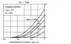
Looking at the ID - VGS graph, for a jfet with Idss = 4.1mA I read Vp (VGS off) <> -0.33V
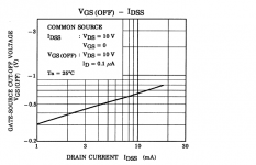
But looking at the VGS(off) - Idss graph, I figure for Idss = 4.1mA, VGS(off) would be <> -0.48V
I am quite confused now so any comment would be a great help.
Looking at the ID - VGS graph, for a jfet with Idss = 4.1mA I read Vp (VGS off) <> -0.33V
But looking at the VGS(off) - Idss graph, I figure for Idss = 4.1mA, VGS(off) would be <> -0.48V
I am quite confused now so any comment would be a great help.
Attachments
I am trying to build a spreadsheet to help me design the bias circuit on a simple jfet gain stage but I did not understand correctly how to read 2SK170 pdf.
Looking at the ID - VGS graph, for a jfet with Idss = 4.1mA I read Vp (VGS off) <> -0.33V
But looking at the VGS(off) - Idss graph, I figure for Idss = 4.1mA, VGS(off) would be <> -0.48V
I am quite confused now so any comment would be a great help.
The graph on the left is asymptotic to the axis and just not drawn well enough nor has the resolution to be accurate for finding Vp. The graph on the right picks an arbitrary current (.1uA) to call "0".
Take a real FET and record Id and Vgs over a reasonable range, you can then use the basic JFET equation to find the Idss and Vp that is a best fit. Even two points like 1mA and 5ma gives a surprising fit. You could try it with the left graph using Vgs = 0 Id = 4.1mA and Vgs = -.1V Id = 2mA and see what Vp best fits these two points.
EDIT - Just use eqation 7 in your reference. I get -.34V for Vp in that graph at 4.1mA Idss. If you plot the whole line with those values it will lie on top of the datasheet graph.
Last edited:
EDIT - Just use eqation 7 in your reference. I get -.34V for Vp in that graph at 4.1mA Idss. If you plot the whole line with those values it will lie on top of the datasheet graph.
Indeed... Thank you for the tip scott 🙂
Or just measure Vgs with a >=1M0 resistor fitted to the Source.
Thank you Andrew.... so you mean maximize RS to get the lowest possible current and fake pinchoff.
Should it work with a grounded gate and a 9V batterie ?
- Status
- Not open for further replies.
- Home
- Design & Build
- Parts
- JFET Basics