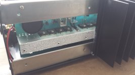

Huum..I'm not sure but I think my amp is mounted differently from what is shown in your pics. I did remove the heatsink as a whole by unscrewing in between the fins. Then I have the PCB with components up and the power transistors flat on the heatsink. I can't reach the solder behind the components. A wider picture below.
http://w3.ualg.pt/~sjesus/IMG_20200210_001250.jpg
http://w3.ualg.pt/~sjesus/IMG_20200210_001250.jpg


use narrow pliers , grab each transistor through hole an one end of tab and wiggle it slightly
one by one , you'll free them all , enough to pry them together from heatsink
one by one , you'll free them all , enough to pry them together from heatsink
ho gosh ! My mistake here is the picture plus another full size. My amp is a PA-5II (maybe the II makes the difference) and it is now clear that your PCBs have solder to the inside (easily reachable) while mine has the PCBs the other way around. The outside looks identical !
http://w3.ualg.pt/~sjesus/IMG_20200210_001250.jpg
http://w3.ualg.pt/~sjesus/IMG_20200210_010503.jpg
Zen Mod, so its brut force ! I'm gona try that. Thanks.
http://w3.ualg.pt/~sjesus/IMG_20200210_001250.jpg
http://w3.ualg.pt/~sjesus/IMG_20200210_010503.jpg
Zen Mod, so its brut force ! I'm gona try that. Thanks.
Hi,
I finally changed C110 on my left channel. Can I test this channel with the power transistors in the air ? In the mean time I scratched the thermal insulation so I think I need a new one. I can't find a long common sheet for all 12 transistors, so I may have to get individual insulation paths. I suppose this is ok ?!
I finally changed C110 on my left channel. Can I test this channel with the power transistors in the air ? In the mean time I scratched the thermal insulation so I think I need a new one. I can't find a long common sheet for all 12 transistors, so I may have to get individual insulation paths. I suppose this is ok ?!
no test without heatsinking
you can use individual pads
if you're not sure of getting the same type as original , change them all , uniformity is important
you can use individual pads
if you're not sure of getting the same type as original , change them all , uniformity is important
Ah ! I was hoping to be able to test whether the activation LED would go off without having to mount the whole thing, in case something went wrong or something else pops up. As a class AB I was hoping that the bias current would be small enough to be turned on without speakers... But ok, that's life.
Regarding the thermal pads, what would be a sufficient thermal conductivity ? Would 12 W / m*K be ok ?
Regarding the thermal pads, what would be a sufficient thermal conductivity ? Would 12 W / m*K be ok ?
more trouble
I know, long time no read...
Here are some news, and not all good. I had many troubles with the power transistors, thermal pads, heat sink, etc, on the left channel (ordering stuff took time). Last week I finally assembled and tested the left channel and... it worked. The LED went off and that channel sounded beautifully (as before). I've done it more carefully with the R channel not to damage anything, and put everything in place today for testing: the LED doesn't go OFF ! Even after 1 hour. May the culprit be on the other nearby caps (C109,C111,C113 - funny enough there is no C112 on the MKII) ? I finally found the closer schematics to my PA5, to be that of the PA7MKII. BTW, C110 is 2.2muF/50V and not the 10muF/35V of PA5 (without MK). Any thought for help here ?
sj
still going....
Hi all,
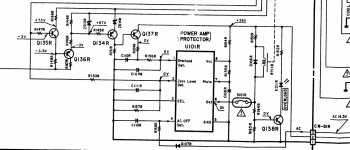
I've now replaced caps C108, C109, C110, C111 and C113 (there is no C112 on PA5II) on the right channel and still protection LED doesn't go off. I've measured pin7 and pin8 of mPC1237 which is the power amp protector IC (see schematics below) and noticed that pin8 is 2.91V and pin7 is 0V (!), while typical values of IC datasheet are 3.4 and 2.06 V. The left channel has 2.9 and 2.2V on those pins. I also noticed that the +36V line is a bit lower at 32.6V (33.3V on the left channel).
Does anyone has a clue on where might be the problem here ?
thanks for any suggestion
sj
Hi all,
I've now replaced caps C108, C109, C110, C111 and C113 (there is no C112 on PA5II) on the right channel and still protection LED doesn't go off. I've measured pin7 and pin8 of mPC1237 which is the power amp protector IC (see schematics below) and noticed that pin8 is 2.91V and pin7 is 0V (!), while typical values of IC datasheet are 3.4 and 2.06 V. The left channel has 2.9 and 2.2V on those pins. I also noticed that the +36V line is a bit lower at 32.6V (33.3V on the left channel).
Does anyone has a clue on where might be the problem here ?
thanks for any suggestion
sj
Attachments
Hi,
Thanks for your suggestion. R155R looks good but to check the solder I have to dismount the whole 12 power transistors, heat sink, etc, etc. A pain in the * !
I wonder if I could turn it on and off for testing with the power transistors in the air ? It would make life a lot easier. I know its risky because I can feel that the left channel heat sink starts to get warm in minutes from fire up, only with the bias current (no input signal).
Btw I checked Q138R and got 0.65 V at the base where it is marked 0 V. This is not a good sign since it means the transistor is open and current is flowing through the overload diode ED11R.
I've also re-checked left channel and I've to correct values in my previous post: 3.3V at pin 8 and 2.2V at pin7 so, very close to theoretical values, according to the muPC1237 datasheet (below). Thanks a lot for your advice.
sj
Attachments
Hi there,
I've been running my tester and R155 is duly connected on both ends, to pin7 and C108. And C108 is connected to pin5 and to 0V. Well, I'm running out of ideas...
I've been running my tester and R155 is duly connected on both ends, to pin7 and C108. And C108 is connected to pin5 and to 0V. Well, I'm running out of ideas...
Probably just as pars suggested. Your going to have to bite bullet and pull it out at and check r155. Also, did you replace the the 1237?
No, not yet. I hate replacing parts completely blind ! But yes, that's maybe the next step. I don't understand why pin8 has 2.9V (below min 3V, and well below 3.4V typical) and pin7 has ~0V, while r154, r155 and C108 seem ok. Maybe I toasted the IC while soldering C108 ?!...
use an alu U bar ,cut 12 piece x transistor ,no insultion if you are bravo end fast to testHi,
Thanks for your suggestion. R155R looks good but to check the solder I have to dismount the whole 12 power transistors, heat sink, etc, etc. A pain in the * !
😉
good idea
Thanks. That's a good idea. Since the power protector does not turns the output relay ON I wonder if the output transistors need to dissipate any heat ? Bias current ? When everything was mounted and turned on, I had the feeling that the left heat sink was getting warmer than the right one. Its summertime so, everything is hot and better not take risks.
I had to order a uPC1237, so now I'll wait for one or two weeks (at best!).
best
sj
Fixed?
I'm curious to know if you ever resolved this issue. I have a Nakamichi PA5 MKII with what sounds like exactly the same issue - but left side. This thread is the only info I have found on it anywhere. I know on mine the C110 cap was not the problem - but have not figured out what to check next. (It would be great to also find a schematic for the PA5 MKII - it does seem to be different than the PA5 which is the only schematic I have found.)
I'm curious to know if you ever resolved this issue. I have a Nakamichi PA5 MKII with what sounds like exactly the same issue - but left side. This thread is the only info I have found on it anywhere. I know on mine the C110 cap was not the problem - but have not figured out what to check next. (It would be great to also find a schematic for the PA5 MKII - it does seem to be different than the PA5 which is the only schematic I have found.)
- Home
- Amplifiers
- Pass Labs
- Issues with newly acquired Nakamichi PA-5 Amplifier