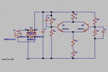
I was thinking that you could use an LTP in a power supply effectively. And naturally, I had to see if I could do anything with my idea with my relatively low amount of experience (sorry...). I was wondering if this idea was any good. I have noticed that it doesn't put out much power and the bias voltages are strongly dependant on the load resistance. This type of supply would probably be included with a product and is not suitable for use with a large range of load resistances (or do they call the load impedaces, or is that what they use for amp output?). i don't think that it is very efficient either... But I'll give it a try anyways!
Here's the schema:
NOTE: I don't really know how to bias an LTP (so please be tolerant)
AND: If you think that the discussion for this will be way over my head, just tell me and I will leave everybody alone...
Here's the schema:
NOTE: I don't really know how to bias an LTP (so please be tolerant)
AND: If you think that the discussion for this will be way over my head, just tell me and I will leave everybody alone...
Attachments
It is always good to have a textbook as reference.The paper back version is cheaper.I know little about transistor biasing but I do know that to simulate sucessfullly you need to input component values which are lacking in this circuit.I think the collectors should be separated individually with it's own resistor and output taken from one of them ( in phase/opposite phase) to a LOAD.Have fun.
I was thinking that I might want to separate the collectors... Well, at least I know that this circuit isn't a failure! I didn't include component values because I don't know much and I didn't want to embarass myself (as much as I hate to admit it). In the circuit, the load is the first resistor coming off of the emitters. Don't have much to say, but I will try and see if I can make it work efficiently. Wish me luck!
Are you trying to make a voltage regulator?
Check out:
http://sound.westhost.com/project15.htm
for a simple capacitance multiplier regulator.
Check out:
http://sound.westhost.com/project15.htm
for a simple capacitance multiplier regulator.
I haven't really thought of taking it as an amplifier, but I guess it works well.
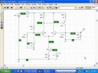
I have another idea. This time the load is connected to the collectors so that it doesn't affect bias voltage as much. The NFB out is an idea I had: This output will be a copy of the actual output. This is sent through a circuit that will rectify it and filter it into a DC source that varies with the amount of ripple after the LTP stage. This is then fed into one of the LTP transistors to increase bias for the underperforming transistor and is a source of negative feedback - hence the name: NFB. Think this will help filter out ripple if I can find an effective way rectify and filter the output?
I have another idea. This time the load is connected to the collectors so that it doesn't affect bias voltage as much. The NFB out is an idea I had: This output will be a copy of the actual output. This is sent through a circuit that will rectify it and filter it into a DC source that varies with the amount of ripple after the LTP stage. This is then fed into one of the LTP transistors to increase bias for the underperforming transistor and is a source of negative feedback - hence the name: NFB. Think this will help filter out ripple if I can find an effective way rectify and filter the output?
Attachments

Why, what nice little toewarmers. Didn't you say you intended to make a PSU of sorts? Where's the output?
It doesn't look like you fully understand a ltp yet. Refer to my picture above.
Generally in a single ended ltp, you will have an input signal connected to the base of one transistor (in this case Q18) and your negative feedback will be connected to the base of the other transistor (in this case Q17). The input signal is a steady voltage reference. R46 and R48 create a voltage divider that divides 10 V down to 5 V at Q18s base. C9 is a filter cap that removes the ripple from the supply so the 5 V is pretty constant with not much ripple. The negative feedback comes in on Q17 and this is directly connected to the load R43.
One of the proporties of a differential pair (ltp) is to keep the bases of the two main transistors the same (Q17 and Q18). So it basically takes the difference between the two bases (Q17 and Q18) and creates an error signal. This error signal is generated up in the collectors of the ltp. In the case of my picture above, I am taking this error signal from R47 and amplifing its current through Q15.
So if the voltage at the base of Q18 becomes higher than the voltage at the base of Q17, the current in R47 will increase causing Q15 to turn on a little more to put more current into the load R43, thus bringing Q17s base voltage back up to the same level as Q18.
So it pretty much in the end steadys itself out. This would be a voltage regulator. This is what I think you are trying to do but am not so sure.
So for all these kind words, would you be so kind as to explain exactly what you are trying to achieve with your circuit. Are you trying to get rid of the ripple so you have a smooth dc from your supply for a load?
I actually have no idea how an LTP works, as I have found out recently. Please don't reply to my posts after this one anymore until I come back and say that I know what I'm doing!
Sorry...
I am trying to make a pretty steady supply. I was thinking that C3 would increase the current ripple at Q1's base and that C2 would increase the ripple at Q2's base in the opposite phase because it is connected to ground. C1 is to sort of filter out ripple before hand so that the bias for the transistors doesn't go crazy. I was thinking that since Ic for one transistor increases while the Ic in the other decreases that the current in Rc would be constant if the circuit was actually doing it's job.
I will try to figure out all this transistor stuff...
- Status
- Not open for further replies.
- Home
- Amplifiers
- Power Supplies
- Is tis a worthy PSU idea?