Good evening,
I've had a little play around in LTSpice this evening and this is the amp that resulted. It's a rather weird one.
Here's an explanation of its operation:
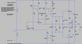
Sziklai pair Q13/Q3 operates as some kind of class-A output stage, if you can call it that. The current through that Sziklai is mirrored by current mirror Q12/Q11/Q6. D1 adds an offset so that the output current of the current mirror is about 40mA lower than its input current. This current is then integrated by C_comp_cfb_1/2. The voltage across those capacitors drives the secondary output stage Q1/Q2/Q9/Q10, which operates as a bipolar current source.
Overall, the circuit attempts to maintain constant current through class-A Sziklai output stage Q13/Q3 (60mA) by injecting an additional current into the amplifier's output via the AB current output stage Q1/Q2/Q9/Q10.
C_comp_cfb_1/2 are deliberately connected to the amplifier's output instead of ground. This results in the Q1/Q2/Q9/Q10 output stage becoming high impedance at high frequencies, allowing the relatively lower-impedance Q13/Q3 stage to take over. This gives the amp an exceptionally good high-frequency response (flat to >1MHz) and improves stability quite a lot.
C_comp_sziklai_opt might not actually be needed, it's just in there for peace of mind. Nobody wants an oscillating amplifier, after all. It doesn't increase THD much.
D2/D3 make setting the quiescent current of the AB current output stage (Q1/Q2/Q9/Q10) very easy and stable over temperature. Thermal coupling between the transistors is not needed. Removing the diodes and using a more standard bias arrangement didn't make much of a difference in THD in simulation.
Of course, the amp has a Vbe drop of offset between its input and output, but that's easy to fix (AC coupling / offset servo), so I'm not going to put it into the simulation for now.
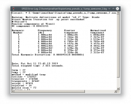
Simulation results:
THD @ 20Vpp, 1kHz, 4 Ohms: 0.000064%
THD @ 20Vpp, 10kHz, 4 Ohms: 0.000091%
Frequency response: flat to >1MHz
My questions are:
Thanks,
Jonathan (aka ttlhacker)
I've had a little play around in LTSpice this evening and this is the amp that resulted. It's a rather weird one.
Here's an explanation of its operation:
Sziklai pair Q13/Q3 operates as some kind of class-A output stage, if you can call it that. The current through that Sziklai is mirrored by current mirror Q12/Q11/Q6. D1 adds an offset so that the output current of the current mirror is about 40mA lower than its input current. This current is then integrated by C_comp_cfb_1/2. The voltage across those capacitors drives the secondary output stage Q1/Q2/Q9/Q10, which operates as a bipolar current source.
Overall, the circuit attempts to maintain constant current through class-A Sziklai output stage Q13/Q3 (60mA) by injecting an additional current into the amplifier's output via the AB current output stage Q1/Q2/Q9/Q10.
C_comp_cfb_1/2 are deliberately connected to the amplifier's output instead of ground. This results in the Q1/Q2/Q9/Q10 output stage becoming high impedance at high frequencies, allowing the relatively lower-impedance Q13/Q3 stage to take over. This gives the amp an exceptionally good high-frequency response (flat to >1MHz) and improves stability quite a lot.
C_comp_sziklai_opt might not actually be needed, it's just in there for peace of mind. Nobody wants an oscillating amplifier, after all. It doesn't increase THD much.
D2/D3 make setting the quiescent current of the AB current output stage (Q1/Q2/Q9/Q10) very easy and stable over temperature. Thermal coupling between the transistors is not needed. Removing the diodes and using a more standard bias arrangement didn't make much of a difference in THD in simulation.
Of course, the amp has a Vbe drop of offset between its input and output, but that's easy to fix (AC coupling / offset servo), so I'm not going to put it into the simulation for now.
Simulation results:
THD @ 20Vpp, 1kHz, 4 Ohms: 0.000064%
THD @ 20Vpp, 10kHz, 4 Ohms: 0.000091%
Frequency response: flat to >1MHz
My questions are:
- Do you think this amp would perform well in practice?
- Is the very low THD just an artifact of the simulation?
- How can I improve it further? (I'd like to keep D2/D3.)
Thanks,
Jonathan (aka ttlhacker)
Attachments

Tempting design, anyhow.
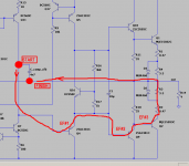
The Q13-Q14 node will make havoc nonetheless, only the cczo 680p and base Q3 as load.
Ccompcfb~# will not act as ideal load for Q6; maybe in simu, not in reality. Better build a proof on wireboard.
Signal is from Q6, so Q16 should by topsyturvy to promote equal ac on both bases of Q10Q9 (very often seen mishap on numerous designs, i've given up already).
Why D2D3 anyhow? Elaborate.
Tempting design, anyhow.
The Q13-Q14 node will make havoc nonetheless, only the cczo 680p and base Q3 as load.
Ccompcfb~# will not act as ideal load for Q6; maybe in simu, not in reality. Better build a proof on wireboard.
Signal is from Q6, so Q16 should by topsyturvy to promote equal ac on both bases of Q10Q9 (very often seen mishap on numerous designs, i've given up already).
Why D2D3 anyhow? Elaborate.
About D2 and D3: As long as the voltage drop across R3,R4 stays low enough, they won't conduct. The operating point of the amp is chosen so that the voltage across each is about 400mV, which causes the diodes to not turn on when only quiescent current is flowing. This results in more than 7 ohms (R1,2,3,4) being in series with the emitters, which causes the quiescent current to be very stable with temperature. At higher currents, the diodes begin to conduct, which prevents R3 and R4 from wasting an excessive amount of voltage.
Q13,Q14 node: Putting a resistor there might make THD quite a bit worse, but I'll give it a try. The current source Q14,Q15 has to stay, however, because it pushes a minimum current through Q13, which makes base current variations of Q3 have less influence on the Vbe of Q13, thus lowering distortion. What kind of havoc do you think that node will create?
C_comp_cfb and Q6: Why isn't that capacitor a good load for Q6? After all, the miller compensation capacitor in a regular opamp VAS does the same thing, it integrates a collector current into a voltage. Please explain. A buffer stage (emitter follower) after c_comp_cfb might be a good idea, though, I'll try that too.
Q16: That one should indeed be replaced with something better. I just put it there to get the amp up and running quickly in the simulation. What do you suggest I should put there? (I don't know what you mean with "topsyturvy", unfortunately.)
Thanks for your feedback!
ttlhacker
Remind yourself: it's an output stage, it needs a front-end if the goal is to make an audio power amplifier with input to output gain of approx 26dB.
When the output swing is low, some power is lost in the 3R3's (~40%), which is considered considerable in general, but no problem because of low voltage swing (a few Watts lost in A mode). When output swing is high, some power is lost in the not-linear diodes to be corrected by the feedback. During normal audio program, the diodes will switch on and off all the time. It is to say the least a unique approach, and maybe a very clever solution. Never seen before, so do build it!About D2 and D3...
A resistor is lineair, a capacitor is another thing. Open for fair appraoch. Let's see what happens in reality....putting a resistor there might make THD quite a bit worse,...it pushes a minimum current through Q13...What kind of havoc do you think that node will create?
Some 18mA is not a minimum current actually.
It is a high Z node (only with rbinQ3) with a 680p cap. That a serious pole to keep in mind. Build!
I'm not sure about this integration claim. I'm from another decade and first thing in my mind with capacitive integration is slewrate. Q6 runs 18mA so that's some 8V/usec max. (C*V=I*t, took 10V swing test)C_comp_cfb and Q6: Why isn't that capacitor a good load for Q6? After all, the miller compensation capacitor in a regular opamp VAS does the same thing, it integrates a collector current into a voltage. Please explain. A buffer stage (emitter follower) after c_comp_cfb might be a good idea, though, I'll try that too.
Granted, but take an pnp instead of a npn. Signal is from Q6 and not from Q7....up and running quickly in the simulation...topsyturvy...
Signal promototes through a bjt from b or e to e or c, never from c to anywhere. If R17 is fixed, have R16 as a 2k2pot and a 1k5 fixed. If R16 is prefered fixed, have R17 as a 470Epot and a 470E stopper.
Keep inmind that the current from Q13 (18mA) and from Q3 (60mA) has to be swallowed by the D2-R3-R2-Q2 compound, and thus differs seriously from the topsection.
And as Ramcres notes, I intuitively agree with that observation.
Yes, the diodes will switch all the time - which is why they have to be relatively fast, 1N400x won't do there. I've used this diode "resistor bypassing" arrangement in other amplifiers in the past, it works quite well!When the output swing is low, some power is lost in the 3R3's (~40%), which is considered considerable in general, but no problem because of low voltage swing (a few Watts lost in A mode). When output swing is high, some power is lost in the not-linear diodes to be corrected by the feedback. During normal audio program, the diodes will switch on and off all the time. It is to say the least a unique approach, and maybe a very clever solution. Never seen before, so do build it!
The base input resistance of Q3 should be around 50 ohms (assuming beta=100), actually, so the node isn't that high impedance after all.A resistor is lineair, a capacitor is another thing. Open for fair appraoch. Let's see what happens in reality.
Some 18mA is not a minimum current actually.
It is a high Z node (only with rbinQ3) with a 680p cap. That a serious pole to keep in mind. Build!
Also, the capacitor actually creates a zero in the overall current feedback path, not a pole, since it couples current from Q13 into the current mirror, bypassing Q3. So it enhances stability no matter how big it is. Even increasing it to 100nF doesn't make the amp unstable. It also creates a dominant pole in the Sziklai's local feedback loop, stabilizing that as well.
So, in the end, that single capacitor stabilizes both feedback loops of the amp.
Since the compensation capacitors are connected to the output instead of ground, you can't actually calculate slew rate like that. You've got 8V/usec on the input of the AB current output stage (between base and output), which has about 0.5 ohms resistance on its emitters, resulting in 16A/usec current slew rate. Across 4 ohms speaker impedance, that's 64V/usec at the output. Plenty, in my opinion.I'm not sure about this integration claim. I'm from another decade and first thing in my mind with capacitive integration is slewrate. Q6 runs 18mA so that's some 8V/usec max. (C*V=I*t, took 10V swing test)
This slew rate problem (as well as stability reasons) is exactly why I chose to connect the compensation capacitor this way, and not to ground. It improves both stability and slew rate over a ground-connected one.
Fixed! It's still NPN, but being driven by a PNP buffer now. Plus 10µF parallel capacitance to ensure proper AC coupling.Granted, but take an pnp instead of a npn. Signal is from Q6 and not from Q7.
Signal promototes through a bjt from b or e to e or c, never from c to anywhere. If R17 is fixed, have R16 as a 2k2pot and a 1k5 fixed. If R16 is prefered fixed, have R17 as a 470Epot and a 470E stopper.
Adding the buffer also eliminated the influence of the non-linear base current of Q9/Q10, which improved things as well. (At the cost of using even more components, of course.)
Oh wow, I totally forgot about that! Fixed as well by adding a matching current sink that drains this current from the output again.Keep inmind that the current from Q13 (18mA) and from Q3 (60mA) has to be swallowed by the D2-R3-R2-Q2 compound, and thus differs seriously from the topsection.
And yeah, this unity-gain amp might have quite a few components... but I don't really see this as a problem. If adding a couple more cheap components improves performance (and doesn't decrease stability), it's absolutely worth it in my opinion.
I will make a prototype PCB over the next few days/weeks depending on when I've got time (I'm currently working on my bachelor thesis). If you've got any more suggestions on how to improve the thing, let me know!
Simulation results:
THD @ 1kHz, 20Vpp, 4 ohms: 0.000019%
THD @ 10kHz, 20Vpp, 4 ohms: 0.000061%
Jonathan
Attachments

I'm seriously baffled... could post every issue in detail, but I go along now.
It is not a true Sziklai however, so... hmm... hmm... hmm...
Slew is trumped by you, by reasoning. Hats off!
Have it a true build, post me pm if, I like it!!!
Boyoboy, so... what's the proper expression?
edit: save the Q7-Q11 node, now you're introducing another pole (?)?
It is not a true Sziklai however, so... hmm... hmm... hmm...
Slew is trumped by you, by reasoning. Hats off!
Have it a true build, post me pm if, I like it!!!
Boyoboy, so... what's the proper expression?
edit: save the Q7-Q11 node, now you're introducing another pole (?)?
Last edited:
If you've got any more suggestions on how to improve the thing, let me know!
I'm on Hiraga's edge, to show colors. Down to bare six bjt's to get same things done.
Unsurpassed sofar in this and the former century.
A challenge.
Read anything about this if possible. I consider anything else as humbug now.
I have a not-so-proper-build H-amp now, and it is flabberghasting. (No protection either on expansive planers/electrostatics!)
Did I write something in capitals, not to scream?
Even with the current sink Q6, absorbing the 60mA from Q3, Q2 has to swallow 18AmA from Q13.
An unbalancd to be balanced challanging enterprise.
All said, now build.
An unbalancd to be balanced challanging enterprise.
All said, now build.
this is why sims are not much good. this amplifier is unity gain as drawn because the input KSC3503 emitter is shorted to the output.
There are quite some issues to clearify what is reasonable in simulation and how things behave in reality. The proof of the pudding is in the eating.
Let's await ttlhacker's follow up.
And let's keep an open mind and pleasure in our mutual diy experience. Even if things proof not viable. Mankind struggling to reach the moon from the primordial mud and such...
Let's await ttlhacker's follow up.
And let's keep an open mind and pleasure in our mutual diy experience. Even if things proof not viable. Mankind struggling to reach the moon from the primordial mud and such...
Current through Q3 has been decreased to about 40mA, Q13 sources another 20mA, which gives 60mA that's swallowed by Q6, so that should actually work out. Some tuning might be required in practice, but a couple of milliamps of imbalance won't kill the thing. Q2 can handle that, as long as it's not significant compared to its ~100mA quiescent current. I'd say it's probably fine even if there's 20mA of imbalance.Even with the current sink Q6, absorbing the 60mA from Q3, Q2 has to swallow 18AmA from Q13.
An unbalancd to be balanced challanging enterprise.
All said, now build.
I guess the prototype will show if that's stable. (I hope it is...)Notice that the 4n7 capacitor is bootstrapped by three emitter followers connected in series
This pole was in there before (C_comp_cfb1/2), I've just consolidated the caps into one when I inserted the additional buffer stage. It's the dominant pole of the current feedback loop.edit: save the Q7-Q11 node, now you're introducing another pole (?)?
I'm currently putting the circuit into Eagle and making a prototype PCB layout for it. (That's faster for me than using stripboard as I can just make the PCB on my CNC mill)
I'll post the results once the thing is built! Might need to buy a few transistors though, not sure if I have the correct types at the moment.
Jonathan
- Home
- Amplifiers
- Solid State
- Is this amp design any good? ("Pseudo-Class-A"?)