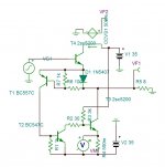
May be I re-invented the wheel.


The circuit is very simple idea. the upper part is just an emitter follower with a current sense diode. As long as the diode is passing a current, T2 swallows the output base current except what R2 limits the bias current 180ma. When the output voltage goes negative the diode passes less current , then the T2 releases more juice to the output base trying to keep the current in the diode constant. By this, the negatve pole modulates itself.
Isn't nice hæ , isn't it.
Attachments
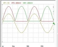
What is trying to keep this current constant? During the negative half, T3 is a constant current source set by R3. How did this plot happen?...trying to keep the current in the diode constant...
The red curve is the current of T4 & the green is T3. The voltages are taken on 0.5 ohm. R3 limits the current about 3A.
The red curve is the current of T4 & the green is T3. The voltages are taken on 0.5 ohm. R3 limits the current about 3A.
That was all already clear to me, T3 curve, T4 curve and R3 limiting the current.
But what is trying to keep this current in the diode constant remains the question, because that is not in control of R3 as it is connected to the +rail and T2 is disconnected by closed D1-T1.
How is the negative current (from load to T3) modulated and not constant as limited by R3? Where does this modulation originate from as measured on R4? What is the signal path during the neg half? Are D1-T1 really closed or feeding this neg signal modulating T2
"The negative pole modulates itself."
I'd say possible patent...
Suppose the T2 is a very slow transistor . If the input suddenly passes to -5v. T4 goes cutoff, the voltage across the sense diode falls , T1 goes cutoff , T2 starts releasing the base current , T3 starts pulling current from the load until it reaches -5v plus some extra current from T4 via the diode. Now the diode reaches the same potential as quiescent operating point that T1 conducts current to T2 ,shouting, thats enough.
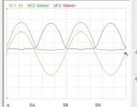
So at a certain point during the negative curve of the input signal, T3 sinks both current from the load and current through D1 from T4. At that point, D1 and T4 switches on again after a short shotoff before this certain point.
It is not a non-switching output stage, but a double switching output stage.
You put me out of balance as I tried to find the signal path that was closed during the short D1-T4 switch off time.
It is not a non-switching output stage, but a double switching output stage.
You put me out of balance as I tried to find the signal path that was closed during the short D1-T4 switch off time.
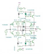
I didn't have the same transistor models, but I found I had to halve R2 and R3 to get good output swing low, and tame T2 with 330pF Miller capacitance to reduce ringing, but it seems to handle 30kHz 25V sine wave fairly well after that. R1 can be tuned for good current matching.
Attachments
So at a certain point during the negative curve of the input signal, T3 sinks both current from the load and current through D1 from T4. At that point, D1 and T4 switches on again after a short shotoff before this certain point.
It is not a non-switching output stage, but a double switching output stage.
You put me out of balance as I tried to find the signal path that was closed during the short D1-T4 switch off time.
It was to suppose only the time of explanition that T2 is very slow. Now if you switch back to a very fast one , if the T4 current decreases slightly , instantly the bias current of T3 will start flowing also from the output , meanwhile T1 and T2 with their combined gain and speed will command T3 to increase the current. This how the amount of bias and the speed are linked so that there is no any crossover . The master follower transistor T4, behaves as if it is class A CCS loaded. T1 remains linear , nonswithing.
Last edited:
I didn't have the same transistor models, but I found I had to halve R2 and R3 to get good output swing low, and tame T2 with 330pF Miller capacitance to reduce ringing, but it seems to handle 30kHz 25V sine wave fairly well after that. R1 can be tuned for good current matching.
I designed this amp today, in less than an hour. It is just born. This is just the feasibility model . I don't have LT simulator , please ,post the schematic.I appreciate your interest .
I designed this amp today, in less than an hour. It is just born. This is just the feasibility model . I don't have LT simulator , please ,post the schematic.I appreciate your interest .

KK,
I spent some hours on this circuit. It's clever and I like it.
However, it has more distortion than a well designed AB bipolar, and it is difficult to make it completely stable at 20KHz. I noticed that to drive the upper device you need a low impedance, so that mandates a driver, I used a C4793. Then it worked very well, but as I said the stability of the lower device drive system is problematic.
This is not to say it's not workable. It has a very good harmonic profile, monotonic and low, but needs work on the lower output drive circuit. I saw a minimum at lower of 67mA, upper 170mA, and quiescent no signal of 180mA. There is no swich-off at any point and the transitions are well controlled.
HD
Last edited:
Maybe not - time for you to name it 🙂May be I re-invented the wheel.
The circuit is a variation on the Taylor White follower.
Some other variations here (the control return path is arranged somewhat differently):
Taylor Source Follower
Note that you can move the sensing diode to the collector of T4: it changes nothing, but it is more convenient.
In some implementations, I have even used the BE junction of T4 as sensor.
Here are some other examples, including error-correction:
Halve the diamond, double the performance!!!
https://www.diyaudio.com/forums/sol...f-follower-cut-leader.html?highlight=unigabuf
Thanks to advises . I developed a similar technique upon diamond output with floating bias supply ( bootstrapped zener) . This is just a quick trial to see if it works . It does reduce the distortion , just a little bit.

https://www.diyaudio.com/forums/attachment.php?attachmentid=842533&stc=1&d=1589089581

https://www.diyaudio.com/forums/attachment.php?attachmentid=842533&stc=1&d=1589089581
Attachments
Last edited:
- Home
- Amplifiers
- Solid State
- Is this a new non switching output stage ?