Looking nice!I think the output part should be three-level. for low impedance speaker systems will be better in terms of distortion...
will be pretty similar to what I simulated and named Cordell -1
Yes, 3EF OPS would be nice. My next project. There is build like that called Wolverine amp. They also use multiple output transistors in parallel for load invariant performance.
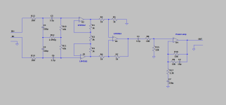
My goal with this particular thread is to stay as close as possible to the original Blameless amplifier concept.
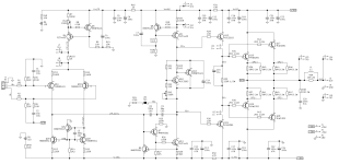
Power supply voltage of 37V which potentially allows for 100 to 130W of power output into 4 ohms load.
Simple CCSs for LTP and VAS.
Simple two transistors LTP.
Improved current mirror for less output offset DC voltage.
Emitter follower VAS with current limiting transistor for easy compensation and nice clipping behavior respectively.
Emitter follower OPS for great stability and decent performance.
All this goodness using SMD components for nice compact board. Better VAS transistors available in SMD packages too.
Last edited:
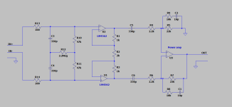
Next iteration is using different output transistors - I figured since I am using TTA004 TTC004 drivers by Toshiba, it will be nice to match them with Toshiba output transistors like 2SC5200 2SA1943.
Added two paralleled output transistors, so technically it is 2EF-2 OPS. 20K distortion were reduced 10 times at full output.
Newly discovered by me VAS and CCS transistors - PZT4401 and PZT4403. Only 40V - which I figured is ok since bias spreader separates DC operation point between CCS and VAS transistors in half with respect to the power rails, which I got at 37V.
So max power voltage cannot exceed 40V. All calculations were done using 37V though.
Adjusted current mirror resistors to be able to work with BC846B transistors as those are affordable and nice performing. Even BC847B should be fine with voltage rating of 45V.
Tried BC847CB/BC857C in simulation and did not make that much of the difference. Only marginal improvement in THD.
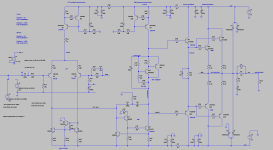
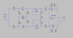
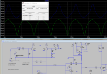
Attached is the schematics.
Added two paralleled output transistors, so technically it is 2EF-2 OPS. 20K distortion were reduced 10 times at full output.
Newly discovered by me VAS and CCS transistors - PZT4401 and PZT4403. Only 40V - which I figured is ok since bias spreader separates DC operation point between CCS and VAS transistors in half with respect to the power rails, which I got at 37V.
So max power voltage cannot exceed 40V. All calculations were done using 37V though.
Adjusted current mirror resistors to be able to work with BC846B transistors as those are affordable and nice performing. Even BC847B should be fine with voltage rating of 45V.
Tried BC847CB/BC857C in simulation and did not make that much of the difference. Only marginal improvement in THD.
Attached is the schematics.
Attachments
Great stuff!
A suggestion: since a lot of the Blameless concept is about crossover distortion, have you done any investigating into this aspect (for example, distortion figures for mid to high frequencies at low output levels - maybe 10mW or similar)?
A suggestion: since a lot of the Blameless concept is about crossover distortion, have you done any investigating into this aspect (for example, distortion figures for mid to high frequencies at low output levels - maybe 10mW or similar)?
I haven't, but adding two pairs of output transistors showed reduced distortion at 20kHz at the max power out levels.A suggestion: since a lot of the Blameless concept is about crossover distortion, have you done any investigating into this aspect (for example, distortion figures for mid to high frequencies at low output levels - maybe 10mW or similar)?
D. Self calls it large signal non linearity distortion.
It would be interesting to test at small output levels - something for the future.
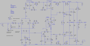
On the practical side, revised schematics to include test points, power LED indicators and added two additional output transistors.
Added test points:
TP1 and TP2 - to measure LTP current
TP3 and TP4 - to measure VAS current
TP5 - before output L-R series network to measure stability
TP6 and TP7 - to measure output
To allow for safe current adjustment two jumpers that disable output transistors completely form the driver transistors are included: JP11 and JP12
Input network will be revised to accept non-balanced signal - todo list.
Attachments
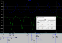
Interesting information I learned recently about setting the current for the driver transistors for the OPS.
In the simulation I can measure waveform for the collector current for the drivers.
By varying resistance from 100R to 470R the current can be increased or decreased respectively.
This results in current dips that are approaching 0.
Meaning the driver no longer is driving output transistors.
As example consider a slide with 470R resistor setting the current to 3.9mA. The load was set 4 ohms. Driver transistors' collector current dipped to almost 0 at 124uA.
In the slide with 100R resistor the current is set to 18mA and from the simulation graph it can be seen that driver transistors' current dipped to 12.79mA.
Doing math we get current needed 5.2mA or more for the driver.
Switching to 2 ohms load changes things significantly in a much worse direction.
Attachments
-
 drivers-collector-currents-100R-18mA.PNG16.7 KB · Views: 79
 -
 drivers-collector-currents-120R-15mA.PNG17.6 KB · Views: 73
 -
 drivers-collector-currents-140R-13mA.PNG17 KB · Views: 65
 -
 drivers-collector-currents-160R.PNG17.6 KB · Views: 70
 -
 drivers-collector-currents-180R.PNG18.1 KB · Views: 76
 -
 drivers-collector-currents-200R.PNG17.9 KB · Views: 74
 -
 drivers-collector-currents-330R-5.6mA.PNG17.6 KB · Views: 79
 -
 drivers-collector-currents-220R.PNG17.5 KB · Views: 62
 -
 drivers-collector-currents-470R-3.9mA.PNG17.7 KB · Views: 70
Last edited:
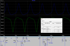
Adding speedup capacitor allows for the smooth current sourcing and sinking.
Value needs to be adjusted based on the current.
In my case the best result was achieved with 200R resistor setting current to 9.2mA and cap value of 2.2uF.
This allowed for 2mA of the current headroom.
Note that if capacitor is added, the current needs to be set higher as capacitor absorbs some of it.
In the previous post it can be seen that 200R resistor allows for 4mA of headroom, but if the capacitor is used, the headroom is reduced to 2mA.
Attachments
Nice work with LTSpice. A while ago Douglas offered a differential input board for the blameless amp. I looked at the web site and didn't see it just now. http://www.signaltransfer.freeuk.com/ I built the Load-Invariant version of the amplifier and It has worked really well for me. I was planning to modify the amp to use it as a transconductance amplifier. I think I had a modification working in LTSpice, but I didn't get around to trying the modification on my amp.

Thanks! I'm still learning and it is a lot of fun!Nice work with LTSpice.
I could use a simple instrumentation amp topology for input buffer that will combine differential signal using three opamps and sends it to the amp.A while ago Douglas offered a differential input board for the blameless amp.
I was also thinking about using actual amplifier instead of the third opamp in the instrumentation amp schematics.
Will sim both, but don;t have time for that yet.
http://www.signaltransfer.freeuk.com/lownoisebal.htm Here is the input board. I missed it when I looked earlier. I think it may be described in the book.
One op-amp is plenty. The instrument amp is overkill and prone to issues with speed and fidelity.
https://en.wikipedia.org/wiki/Differential_amplifier#/media/File:Op-Amp_Differential_Amplifier.svg
If R1, R2, Rf, Rg are all equal then the gain is 0dB, unity, but you can have gain = (Rf=Rg)/(R1=R2). You can add a load resistor to the + input to match the - input impedance. You can add a load resistor across both inputs. Also common in audio is two inverters where the second one is also a summing amp.
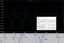
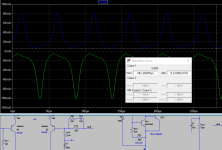
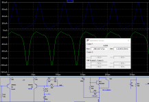
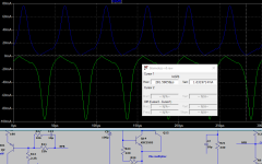
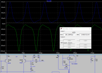
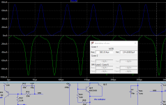
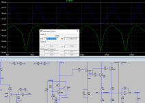
Finally got around to do the phase margin analysis.
Compensation values were adjusted accordingly.
Verified for square step response as well.
Summary of compensation:
Compensation values were adjusted accordingly.
Verified for square step response as well.
Summary of compensation:
- Two pole compensation across VAS
- Series RC network across the feedback resistor aka phase lead cap
- Series RC network across LTP output. Cap values of >100p resulted in excessive 20kHz distortion. Reducing cap to 22p still adds some HF distortions but a compromise.
- Series RC networks at the VAS output. This one does not seem to change that much. Or maybe I am missing a way to measure it.
Attachments
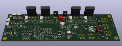
pzt4401/03 are SMD in SOT223 package.
I am using all SMD components except driver and output transitors.
I am using all SMD components except driver and output transitors.
What do you think about MJE15034/35 for replacement?3503/1381 won't overheat? they are not very powerful as far as I remember ... 340/350 is more powerful like .. well, or as always popular 2SA1837/2SC4793
In the simulation I run my VAS at 8mA which for 37V psu voltage shows dissipation of 270mW for the CSS side and 277W for the VAS transistor itself.
PZT4401/03 datasheet specifies dissipation of 1150mW for the SOT223 mounted on 1cm^2 pad.
Around four time less then the max power dissipation rating I think should be fine.
I am using A1381/S3503 as drivers and I simulated their collector currents to make sure they don't go to near 0mA.
Running drivers at 9mA in the simulation shows current dips down to 3.4mA while input is fed 20kHz at 2.82V peak. Load was 4 ohms.
I am concluding from the simulation that A1381/S3503 are capable of driving two two pairs of 1302/3281 output transistors.
Power dissipation for KSC3503 is 586mW and for KSA1381 it is 539mW.
From the datasheet max power dissipation is 7W.
Should be plenty of headroom.
Now, this is all done in the simulation and the real world circuit might show otherwise, but for now I am thinking I should be fine using A1381/S3503 as drivers.
I am not opposed to use more powerful drivers either. Like TTA004/TTC004 or since MJE15032/33 are not in stock on Mouser, MJE15034/35.
Honey Badger uses MJE15032/33 to drive three output pairs and they seem to know what they are doing.
Attachments
Last edited:
15032/33, as for me, are more like output transistors than output transistor drivers. somewhere in some circuit I saw them as output transistors. I put them instead of those in the circuit in apex-20 and got the problem of excitation of the circuit. increased the capacity of the miller, then it worked ... that is, they are slow or something or something ...
- Home
- Amplifiers
- Solid State
- Is there a simple one-to-one simulation for Blameless amplifier in LTspice?