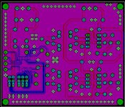
its a layout for an pcm1716, but that´s not of interesst as I wrote it. What´s important for me is, are the via´s between solder and bottom ground layer any good? I mean, normally 2 ground layer´s aren´t the best, but i thought that "some" via´s could solve the problem of differentail voltages and currents between them...... AND: ground planes look sooooo professional ;-), beside that my etching solvant holds longer cause fewer copper to remove......
thanks...
thanks...
- Status
- Not open for further replies.