Jaka Racman said:Hi Wheberth,
1) I suppose you mean over and undershots of source connection of the driver. No, buffer will not prevent that, it can actually make things worse because of faster switching transients of the power mosfets. The best way to prevent this is compact layout (minimum loop area) of the power stage, kelvin connection of the driver circuit (driver circuit and power circuit are connected only at the source pin of the power mosfet). Sometimes gate resistor is put into source connection instead of the gate connection.
2) ZTX618 and ZTX718 seem to be electical equivalents of FMMT devices in TO92 case. For driving mosfets you could also use lower voltage (15V devices). Check Zetex page.
3) Buffers will certainly improve switching times and will also lower on state losses, because of lack of gate turn on tail. How many percent higher efficiency will that bring is hard to tell.
4) I have no personal experience with this one. On paper it looks good and certainly worth trying. I have very good experience with IR2110 devices which I use almost from the beginning of their production. But I was disappointed with early batch of single 8pin drivers (IR212&IR2125) that had short circuit protection. Their propagation delay was too much dependant on amplitude of the drive signal, so I never tried them again.
Best regards,
Jaka Racman
Hello Jaka. I like the IR211x very much as well. I have been following with interest the idea of buffering the IR211x. I found an alternate method has worked well for me. I use a dual SO-8 packaged MOSFET like the IFF7343 or the IRF9952. They do shunt overshoots through their body diodes, so I have not had failures that way when using the MOSFETs as source followers.
The output of the N-ch drives the gate through a resistor for turn-on, while the P-ch can go straight to the gate for turning it off. The peak current of the IR7343 is around 30 amps with short rise and fall times. The inputs of the IR7343 do not need resistors in this case, I'd say.
Attachments
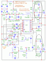
Hello, subwo1. That's a halfbridge offline smps, isn't it?
Does it work well? What is its power rating and output voltage? Do you have some photos or something to see it?
I was fighting with that things for some time and I am curious!
BTW: R9 must get reeaally hot, doesn't it?
Best regards,
Pierre
Does it work well? What is its power rating and output voltage? Do you have some photos or something to see it?
I was fighting with that things for some time and I am curious!
BTW: R9 must get reeaally hot, doesn't it?
Best regards,
Pierre
Hello Pierre, yes, the component values are more for 120VAC operation. R9 draws about a couple of watts then. For more power to the primary control circuits, or for 220VAC operation, it may be better to use a small supplemental power source. Yet, if the switching frequency is low enough, the value of the resistor can be increased since the power consumed by the MOSFET drive then goes down. Another option is to use a start-up "bootstrap" circuit, but I am not a fan of that technique. A small 100ma 50/60 hz transformer is easiest--rectified and regulated with a 78L15. A mini flyback circuit can be a good possibility (I am drawing up a circuit diagram of one of those still.), or a couple uF capacitor with a series resistor to supply line AC to some rectifiers.
I think it works well, but since it is my baby, I would be biased. Alas, I have no pictures. I have had plenty of help from some kind folks who have worked out PCB layouts. You might like to read all my ramblings about it in the group linked below (I use the files section for notes and diagrams.) where we discuss various options about it and all other aspects of various topologies including ones by other designers as well. Best Regards.
I think it works well, but since it is my baby, I would be biased. Alas, I have no pictures. I have had plenty of help from some kind folks who have worked out PCB layouts. You might like to read all my ramblings about it in the group linked below (I use the files section for notes and diagrams.) where we discuss various options about it and all other aspects of various topologies including ones by other designers as well. Best Regards.
Thanks, subwo1.
I will read the forum messages, it seems quite interesting. I hope to be able to give some useful ideas.
BTW: What is the power level that your are getting reliably?
About the voltage, sorry, I hadn't seen the 12V zener for the overvoltage protection 🙂
Pierre
I will read the forum messages, it seems quite interesting. I hope to be able to give some useful ideas.
BTW: What is the power level that your are getting reliably?
About the voltage, sorry, I hadn't seen the 12V zener for the overvoltage protection 🙂
Pierre
You're welcome. I like suggestions and try to evaluate them.🙂 Some members do provide good ideas, too. I would say that I am not the most skilled one of the group.
I have one running a mini dehumidifier which consumes 120 watts. I have bench tested various prototype versions at several hundred watts.
I have one running a mini dehumidifier which consumes 120 watts. I have bench tested various prototype versions at several hundred watts.
Hi!
Hello Tiki! I also think the max. 'pulsed' GATE current is maybe infinite in theory, if there is no inductrances and resistances of the tracks. The Gate-Sopurce is a capacitive nature load and the peak current is only limited by the tracks' and the leads' inductance and resistance. But don't forget, these inductances and the Gate capacitance are connected parallel through the resistive losses for alternating currents (AC), and therefore can cause ringing. You can calculate the maximum apllicable charging and discharging current on the basis of pole goodness (QP) in order to avoid the ringing (in Control Technic aspects). But you also can do a simulation in the sight of R, L, C. Clearly: The resistance between the driver and the Gate is needed for avoid the ringings because of the tracks' and the leads' inductance, and for limiting the heat dissipation of the driver. If there is no resistor, all the energy stored in the Gate's capacitence is dissipated on the driver's internal FET's Rds/ON/ in every charging and discharging cycle.
What about the amp.?
Hi Wheberth! The antiparallel diodes is always necessary for the FETs driving inductive loads. The intenal parasitic diode is not useable for this purpose. This diode is come from the MOSFET structure and leading technique. Under the manufacturing either shorting the internal BJT structure's Base and Emitter and bind the internal body diode or don't connect the body diode to the Source, but leave the BJT can work. The manufacturers choose the first one. So you shouldn't reckon with the BJT turns on, but the body diode is connected antiparallel with Drain and Source. This p-n junction is made for provide the majority charge for cunduction, after the inversion layer is evolved. This shouldn't be used in forward by chance in low frequency applications, because the charge stored in the opened p-n junction can diffuse slowly, the p-n junction will be open for a long time under the reverse voltage. So, if you use the FETs with inductive load without external fast freewheeling diodes at high switching freqvency (n*10 kHz for the FETs nowadays), there will be very high (!) current pulses under the transition, which will cause a huge oscillation in the supply rails (and also overvoltages), and EMC caused excitation in the other circuits. Maybe the drivers and FETs can't survive this shock!
You can use paralleled MOSFETs with common Gate resistor too. If the drivers is not isolated, you should also connect the GND through a ground plane. The ground plane's purpose is to minimize the inductance (and also the resistance) between the connections.
Good luck!
Gyula
Hi Gyula,
good to hear from you!
Thank you for the explanations. I felt the heat dissipation really, when I started the modified (self oscillating) heater control the first time. It run at approx. 2MHz without any gate resistor. Bringing it back to 500kHz, it stayed cool.
"What about the amp?" Awkward question. The UcD180 version is still not complete and I stopped the "private" development for a while.
Regards, Timo
good to hear from you!
Thank you for the explanations. I felt the heat dissipation really, when I started the modified (self oscillating) heater control the first time.
It run at approx. 2MHz without any gate resistor. Bringing it back to 500kHz, it stayed cool."What about the amp?" Awkward question. The UcD180 version is still not complete and I stopped the "private" development for a while.
Regards, Timo
What type of heater did you make? I think you didn't think about an anagramma? If I were you, a heater can be made at 5 MHz with proper dead time and few ns of current rise and fall times, but maybe a few kHz is also enough. Maybe, at 5 MHz class-D was similar to class-A megahert signal generator. 
I should go to learn. Hi! It was good to hear from you. I thought about your last amp. project.
Gyula
I should go to learn.
Hi! It was good to hear from you. I thought about your last amp. project.Gyula
Look here.
The heater is a platinum layer on 20mmx3mmx0.5mm Al2O3 substrate, used for gas concentration and flow sensors with response times in the ms-range. The temp must remain stable within a few K.
Unfortunately I do not know exactly, what you mean with the anagramma. The heater is needed, the hot driver not. 😀
Timo
- Status
- Not open for further replies.
- Home
- Amplifiers
- Class D
- IRFB52N15D Bridge