Hi Guys!
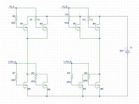
I´d like to know what do you think about a full bridge with 8 IRFB52N15D mosfets. I will use two IR2010 MGD and the dead time will be inserted by a discrete circuit. This circuit need to be able to supply at least 2kW into a 1 ohm load. I´d like to know also if do you know any overcurrent/short-circuit protection.
Sorry about my english!
Thanks
Attachments
i like irfb52n15 using, but you need only 100v mosfets yet. As far as i know at the such power if PCB isn't optimal implemented (that's usual for the first 10 attempt at least;-) ir2110 can work not so much robust. To prevent chip damage put the schotky between Vs-HO and COM-LO. Please keep equal all the gate resistors! 🙂
And what do you think about IRFP90N50D mosfet instead 2 x IRFB52N15D Because I'd like to get 2kW into 4 ohms too.
About dthe MGD i will use IR 2010 not 2110.
Thank you Ivan
About dthe MGD i will use IR 2010 not 2110.
Thank you Ivan
2010 or 2110 no matter,IMHO..
http://ec.irf.com/v6/en/US/adirect/...domSendTo=byID&domProductQueryName=IRFP90N50D
Number of products found: 0. 😕
http://ec.irf.com/v6/en/US/adirect/...domSendTo=byID&domProductQueryName=IRFP90N50D
Number of products found: 0. 😕
IRFP90N20D is too heavy, actually IRFB52N15 (singles in the H bridge) will give 2800w@4ohm.
PS: Folks, i'm still misunderstand such power requirements as UcD700/1000, or your 2000w@4ohm.. really, maybe i'm not so young (37y.o.) or something other
PS: Folks, i'm still misunderstand such power requirements as UcD700/1000, or your 2000w@4ohm.. really, maybe i'm not so young (37y.o.) or something other
Hi,
another thing that I can recommend is use of complementary emiter follower pairs as buffers on outputs of IR2110. FMMT618 and FMMT718 from Zetex are highly recommended.
Best regards,
Jaka Racman
another thing that I can recommend is use of complementary emiter follower pairs as buffers on outputs of IR2110. FMMT618 and FMMT718 from Zetex are highly recommended.
Best regards,
Jaka Racman
Jaka Racman said:Hi,
another thing that I can recommend is use of complementary emiter follower pairs as buffers on outputs of IR2110. FMMT618 and FMMT718 from Zetex are highly recommended.
Best regards,
Jaka Racman
Hi, can you tell me why that would be beneficial? Is it because a FET output stage doesn't have a constant output impedance?
IVX, such power is good for driving motors with, this way after you go deaf you can still use it for something 🙂
Hi Chris,
IR2110 output stage is unsymmetrical, upper driver is source follower, while lower driver is common source. This results in relatively slow gate rise (large tail) times and moderate gate fall times with large Mosfets. At 400kHz typical class D switching frequency those times are too slow and also power dissipation in IR2110 would be to high, since combined gate resistor is 2.8 Ohm which is even lower than 3 Ohm (IIRC) channel resistance of internal drivers. I use IR drivers with relatively large IGBTs with 2.2 Ohm gate resistors and rise and fall times are improved with emiter follower pairs. Those SOT23 devices from Zetex can source and sink 12A pulse current which is considrably more than 2A specification of IR driver alone. If you are interested I can post some scope pics of gate signals with and without buffers on Monday.
Best regards,
Jaka Racman
Hi Jaka,
Thanks for the explanation.
Zetex has a number of devices in the same general category which look good, but the ones you mentioned in question do seem like the defacto standard for driving mosfets with, it would be nice to see them in action, so yes I'm interested, if it's not too much trouble those scope pics would be educational.
I've noticed they have slightly lower power dissipation capability over other comparable Zetex BJT's but they sport lower Vsat amongst the higher current/beta ones. I'm using them in my current "design".
I can't help but think, having to buffer the driver seems to negate the purpose of having one, but I guess you still get a very fast and efficient level shift out of it.
Best regards
Hi,
who does know a spec of max. pulsed _Gate_ current? Is it infinite? I don't believe, but I cannot find it in the manufacturers datasheets.
The scope pictures would be interesting for me too.
Thank you in advance,
Regards, Timo
who does know a spec of max. pulsed _Gate_ current? Is it infinite? I don't believe, but I cannot find it in the manufacturers datasheets.
The scope pictures would be interesting for me too.
Thank you in advance,
Regards, Timo
I will take a guess at it and say, yep, it's infinity, for the sake of argument.
Actually it's limited only by how fast you want it to switch.
I would say due to other constraints, like Vgs breakdown, gate resistance, package dissipation..... if there is some limite it's likely impossible to reach it and therefore goes unmentioned.
IXYS has gate drivers good for 20 amps btw. They use them to switch at 5Mhz in a resonant switched class d ref design.
Hi Jaka Racman,
I have some questions for you! Can you help me? (Sorry about my english)
1 ) Do the BJT buffer helps to avoid damage of gate driver due to overshoots and undershoots from mosfet switching?
2 ) Are there thru hule BJT´s that can be used instead ZETEX smd ones?
3 ) Using this BJT driver can I improve amplifier's efficience?
4 ) What do you think about IR 2010 mosfet driver?
5 ) I'd like to see the scope pics!
Thank you!
Best Regards
Wheberth
Hi Wheberth,
1) I suppose you mean over and undershots of source connection of the driver. No, buffer will not prevent that, it can actually make things worse because of faster switching transients of the power mosfets. The best way to prevent this is compact layout (minimum loop area) of the power stage, kelvin connection of the driver circuit (driver circuit and power circuit are connected only at the source pin of the power mosfet). Sometimes gate resistor is put into source connection instead of the gate connection.
2) ZTX618 and ZTX718 seem to be electical equivalents of FMMT devices in TO92 case. For driving mosfets you could also use lower voltage (15V devices). Check Zetex page.
3) Buffers will certainly improve switching times and will also lower on state losses, because of lack of gate turn on tail. How many percent higher efficiency will that bring is hard to tell.
4) I have no personal experience with this one. On paper it looks good and certainly worth trying. I have very good experience with IR2110 devices which I use almost from the beginning of their production. But I was disappointed with early batch of single 8pin drivers (IR212&IR2125) that had short circuit protection. Their propagation delay was too much dependant on amplitude of the drive signal, so I never tried them again.
Best regards,
Jaka Racman
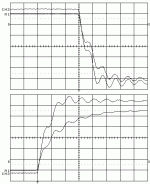
Hi,
here are scope pictures of buffered and unbuffered IR2110 driving 600V/50A IGBT. Time scale is 50ns/div and voltage scale is 2V division. Please note that ringing is due to the test jig (7cm of driver signal path with 2 connectors in between). Interesting fact is that final gate voltage is 1V higher with buffered driver at the same supply voltage.
Best regards,
Jaka Racman
Attachments
Hi,
Thanks alot for those. It's very enlightening to see how weak the driver IC on its own is.
Regards
Chris
Thanks alot for those. It's very enlightening to see how weak the driver IC on its own is.
Regards
Chris
Jaka:
Please have a look at these waveforms I took last saturday. It is a IR2110 unbuffered and with 10 ohms resistors and schottky in antiparallel.
http://www.diyaudio.com/forums/showthread.php?threadid=46560&perpage=10&pagenumber=12
(post #116)
(Lower one is the high side mosfet). The mosfets are Onsemi's NTP35N15 (150V, 37A, 50mOhm).
Scale is 5v/div, 500ns/div. (The waveforms are not aligned in time as they were taken at different moments)
It is too slow, isn't it? I reduced the gate resistors to 6 ohms but haven't taken any pictures yet.
However, the switching signal has 50ns rise/fall times and looks perfect with no ringing, etc.
Hi Pierre,
yes, your waveforms are a bit slow and could be improved with buffer. However, by doing so you might also open can of worms. By faster gate signals you wil get faster bridge transition times and maybe some spikes and ringing which could interfere with feedback. I think that gate rise and fall times somewhere in the 100ns region are fairly good compromise between speed and interference.
Best regards,
Jaka Racman
Edit: I have just seen that you use 40MHz probe. It might be a bit slow to show 10ns wide spikes or 100MHz ringing typical of faster transition times, so your actual waveforms might not be so clean as you think. But I would not worry about that.
Hi Jaka,
Can I drive the mosfets from buffered gate driver without a gate resistor? (Qg=2 x 180nC)
If I speed up FET´s rise an fall times, I will need to place schottky diodes antiparalleled with mosfets (IRFP90N20D)? When I need to use that diodes?
About the PCB layout, wide tracks are problem?
In my case the negative rail are GND (non symertrical PS), Can I connect all GND points (of power and control circuit) to the ground plane?
Thank you.
Hi Wheberth,
In principle you can drive mosfets without gate resistor, but in this case some overshot and maybe ringing on gate signal is almost guaranteed. I use 2.2 Ohm gate resistors and in one case even 0.5 Ohm, but I use them. And like I said I do not think there is much gain by going much below 100ns for gate rise and fall times.
I do not see any need for paralleling schottkys. 100V schottkys have large leakage current and voltage drop that is not much lower than that of the internal diode. So it is a question if the frewheeling current would actually divert to them. Plus you layout would be more difficult and prone to ringing.
Wide tracks are no problem, just keep the loops with main circulating current with minimum area. That often means lying track with return current on opposite layers of the PCB directly below or on top of the original track, even if the resulting track is a little longer. Using ground plane is a good idea, but you must be sure that you have minimum voids in it.
Last I would recheck your choice of power mosfets. Your solution looks like overkill. You might get low Rdson losses, but your switching losses will be skyhigh. IR is a good company and makes very robust mosfets. But I think that Fairchild now produces mosfets with best figure of merit (Rdson/Qg). You might beter use single mosfet instead of two paralleled.
Best regards,
Jaka Racman
- Status
- Not open for further replies.
- Home
- Amplifiers
- Class D
- IRFB52N15D Bridge