Hi,
did some attempts at reducing gate-source voltage ringing and half-bridge center tap ringing by increasing the value of the gate resistors from 10 ohm R0805 SMD to around 22..24 ohm R1210 SMD. Current consumption (at no load) also dropped after soldering in new gate resistors.
Not sure if I've overdone it, though. 22 ohm for gate resistance sounds like quite much...?
The waveforms look a bit on the soft side, too. Although I've no idea if that actually is ok 🙂
Anyone mind having a short glance at the oscilloscope screenshots?
http://users.tkk.fi/~jwagner/electr/subw-digiamp/fluke/
mainly at the last pics? Do you see any problems there?
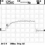
Especially screen 12: upper fet Vgs, rise from 5V to 12V in ~400ns, and last screen 15, halfbridge centertap to ground.
Does the last screen still look ok for class D purposes, or is that way too slow switching?
The setup is roughly:
2-layer halfbridge PCB with two IRFB31N20D's, 12V gate drive supply, PWM at 350kHz, BYM26C 30ns bootstrap diode for IR2110. Each of IR2110 outputs controls a UCC37322 9A peak SMD mosfet driver, which drive one fet through a SMD gate resistor with antiparallel schottky BAT85. Used lab bench supply for rails, adjustable 0..~70Vdc, that is halfbridge eats single supply GND+Vrail and not any symmetrical dual supply.
IRFB31N20D: "TO-220 31A 200V 0.08ohm hi-freq SMPS MOSFET, typ 70nC Qgate @ 160V, typ 30ns switching", http://www.irf.com/product-info/datasheets/data/irfs31n20d.pdf
Many thanks for your input! 🙂
- Jan
did some attempts at reducing gate-source voltage ringing and half-bridge center tap ringing by increasing the value of the gate resistors from 10 ohm R0805 SMD to around 22..24 ohm R1210 SMD. Current consumption (at no load) also dropped after soldering in new gate resistors.
Not sure if I've overdone it, though. 22 ohm for gate resistance sounds like quite much...?
The waveforms look a bit on the soft side, too. Although I've no idea if that actually is ok 🙂
Anyone mind having a short glance at the oscilloscope screenshots?
http://users.tkk.fi/~jwagner/electr/subw-digiamp/fluke/
mainly at the last pics? Do you see any problems there?
Especially screen 12: upper fet Vgs, rise from 5V to 12V in ~400ns, and last screen 15, halfbridge centertap to ground.
Does the last screen still look ok for class D purposes, or is that way too slow switching?
The setup is roughly:
2-layer halfbridge PCB with two IRFB31N20D's, 12V gate drive supply, PWM at 350kHz, BYM26C 30ns bootstrap diode for IR2110. Each of IR2110 outputs controls a UCC37322 9A peak SMD mosfet driver, which drive one fet through a SMD gate resistor with antiparallel schottky BAT85. Used lab bench supply for rails, adjustable 0..~70Vdc, that is halfbridge eats single supply GND+Vrail and not any symmetrical dual supply.
IRFB31N20D: "TO-220 31A 200V 0.08ohm hi-freq SMPS MOSFET, typ 70nC Qgate @ 160V, typ 30ns switching", http://www.irf.com/product-info/datasheets/data/irfs31n20d.pdf
Many thanks for your input! 🙂
- Jan
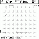
The drain to gnd switching voltage looks ok - it is a bit on the soft side, as you noted, and that is partly because of the gate resistors you're using. It would be nicer if the gate charge voltage were a little smoother, but it looks like the gate rises about 5V above the source and stays there once it gets past that little hiccup so the fet is definitely turned on. You may want to try decreasing the value little by little to speed up turn on and decrease resistive losses in the fets while making sure that the gate voltage stays above the threshold like it does now. Basically fine tuning what you've already shown is working 🙂
Jan,
I'm not certain I understand exactly what is on the Web site, but it looks like the gate to source voltage is ringing way too much in the first few traces. In the later ones, you have really slowed things down. My guess is that you have too much inductance (long leads, not twisted together or poor Vcc bypassing, or whatever) in the gate circuit. Fix that first.
The data sheet shows switching times for Rg=2.5 ohms. Clearly you don't need to go that low, but 22 seems pretty high. Switching losses of the MOSFET are a function of how fast it switches so you don't want Rg to be too large.
Rick
Thanks for your input! Gate drive copper tracks are short and on top layer of the pcb, ~6mm total length from SMD UCC37322 driver to fet gate and a ~6mm ground return track parallel to that gate track (1..2mm spacing between them). 6mm length mainly because of R1210 sized SMD resistor.
Also, the gate drive Vcc supply to GND's waveform directly at UCC37322 pins is very stable and there is no ringing.
Somehow the ringing is only on the side of the mosfet gate pin i.e. after the gate resistor??
Puzzling...
Also for some reason IR2110 + UCC37322 chain has an odd logic signal propagation delay mismatch. Somehow turn-off has more delay than turn on. Leading to that one mosfet will be started to switch on ~50ns before the other is starting to switch off. So large gate resistors obviously helped, and are necessary, otherwise there's 50ns++ time for shoot-through.
Arrgh.
Will have to invent some way to add 50ns turn-on delay to the logic level signals.
Hey is anybody selling "this MOSFET PWM board works till 350kHz 35Vdc" boards for prototyping?
- Jan
- Status
- Not open for further replies.