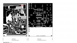
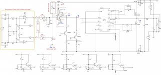
PCB layout
storm in the desert 🙂 and storm in loudspeaker when it will work in bridge mode
btw: why do you want to use 63 V rating capacitor for bootstrap
47 uf 16 V is enough,voltage do not exceed IR2110 supply
storm in the desert 🙂 and storm in loudspeaker when it will work in bridge mode
btw: why do you want to use 63 V rating capacitor for bootstrap
47 uf 16 V is enough,voltage do not exceed IR2110 supply
Attachments
Last edited:
yes,this is correct for low-side not hi-side becouse this pulse to -vcc.
Unfortunately you've already developed PCBs.
A) I do not agree to use lm360 in this configuration becouse output is TotemPole. (You analyze when lm360 close to GND.
B) in this circuit lm360 has disproportionate conversion-time (very fast) this is good, but for others scheme.(complex layers on pcb required)
I think it moves too far out dc offset. (after 30 minutes)
also .. thd is like the sea!
fewer problems if you use a lm319D + HF4070 and 2 trans, jumping for negative voltage-Vcc.
After attach diagram to show you.
hello,
i think you are wrong,
voltage between high side gate capacitor can not exceed mosfet voltage gate rating.(+-20 V),mosfet will blow
i'm using 47 uF 16V tantalum
take a look with a simulator,i use LTspice,it clearly shows that voltage does not exceed 12 V (IR2110 supply - bootstrap diode)
i've let the amp running for 4 hours without signal,offset is still -50 mV,floating analogic input and same impedance on each feet of LM360 seems to be a good choice.
Attachments
Last edited:
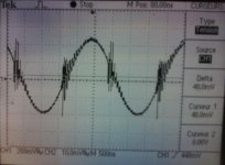
offset rising up
a new problem occurs.
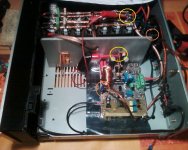
pcb is now mounted on heatsink
carrier frequency drop down ( 400 KHz to 300 KHz ) and offset was +60 mV
i made a shunt between heatsink (close to MOS ) and 0 V capacitor bank.(as shown below on first picture )
frequency reach normal value, 400 KHz but offset has increase...
note that the - speaker is not taken on PCB,directly link to star ground to avoid comon impedance on board.
do i have to insert a capacitor on the other foot of the comparator to cancel offset ?
a new problem occurs.
pcb is now mounted on heatsink
carrier frequency drop down ( 400 KHz to 300 KHz ) and offset was +60 mV
i made a shunt between heatsink (close to MOS ) and 0 V capacitor bank.(as shown below on first picture )
frequency reach normal value, 400 KHz but offset has increase...
note that the - speaker is not taken on PCB,directly link to star ground to avoid comon impedance on board.
do i have to insert a capacitor on the other foot of the comparator to cancel offset ?
Attachments

Last edited:
I'm sorry to say that but your circuit is only useful as a first experience with self oscillating class D. It's far from good enough if you want to do a real amplifier, it lacks everything.
The modulator is mostly useless, it does not have any gain for THD or offset correction, or any immunity against external signals above the audio band, that will disturb the amplifier. Input op-amp is wasted.
The power stage is very precarious too, it suffers from strong ringing that will disturb the own amplifier and other channels near, particularly when radiated by speaker wiring, and there are no protections against overcurrent or short circuit either.
hello,
I'm sorry for the joke that I did.
I was available, imagine how much time you devoted to your amp.
I thought you were laughing!
You too can try to understand that the problems you encounter can not be seen individually. many little things you have to adjust.
if I find time these days, I'll give you some tips to improve your Amplifier.🙂
EVA thanks for reply and argue,a way to motivate
i 've fixed the offset problem,only 62 mV in every case with a carrier frequency =390 KHz
i've try many ways and found out how to solve this.(no capacitor )
the ringing of carrier will be attenuated,i've insert two 47 pF on comparator feet ,no need of these
I'm sorry to say that but your circuit is only useful as a first experience with self oscillating class D. It's far from good enough if you want to do a real amplifier, it lacks everything.
i know that,this is my first attempt with class d,i've build several A,AB amplifier,very easy to setup.
The modulator is mostly useless, it does not have any gain for THD or offset correction, or any immunity against external signals above the audio band, that will disturb the amplifier. Input op-amp is wasted.
the analogic gain was 4:1 at first try,sensitivity was too high,i've decided to decrease gain for this reason
The power stage is very precarious too, it suffers from strong ringing that will disturb the own amplifier and other channels near, particularly when radiated by speaker wiring, and there are no protections against overcurrent or short circuit either.
purpose of this this amp is only for fun building and for home application,no need over current protection,a DC speaker protection will be insert,speaker wire radiation does not exist with BF,all my BF amp works like this,no hum,no hiss.
i 've fixed the offset problem,only 62 mV in every case with a carrier frequency =390 KHz
i've try many ways and found out how to solve this.(no capacitor )
the ringing of carrier will be attenuated,i've insert two 47 pF on comparator feet ,no need of these
Attachments
Last edited:
I was feeling like telling you some tricks to make the amplifier more "commercial grade", but if it's ok for you as it is, then it's ok for me too 🙂 Then again, these tricks would have required a complete redesign 😉
hi, EVA
i've understood that you are engineer,class d theory and practice does not have secrets for you.
i am still trying to make this PCB working.maybe i will come back to AB class amplifier.
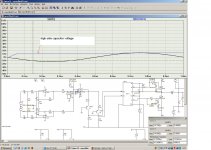
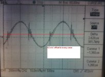
i've try THD measurement, H3 is very bad,and thd is bad too
overall gain is too low ~12
i will increase analogic gain to reduce THD,offset is correct now (+48 mV)
very bad measurment below
i've understood that you are engineer,class d theory and practice does not have secrets for you.
i am still trying to make this PCB working.maybe i will come back to AB class amplifier.
The modulator is mostly useless, it does not have any gain for THD or offset correction, or any immunity against external signals above the audio band, that will disturb the amplifier. Input op-amp is wasted.
i've try THD measurement, H3 is very bad,and thd is bad too
overall gain is too low ~12
i will increase analogic gain to reduce THD,offset is correct now (+48 mV)
very bad measurment below
Attachments


Last edited:
Some hints:
Remove ringing from the output, it adds THD and can cause the amplifier to oscillate at the ringing frequency and self destruct. Output capacitor inductance is a problem. This may require redoing the power stage, adding RC snubbers and SMD ceramic capacitors.
Move the modulator into a daughter PCB with SMD and continous ground plane. The spatial plane of this PCB should be free from EMI (perpendicular to main PCB and to inductor radiation plane.
Change the circuit into post-filter feedback.
Add differential feedback from the output to reduce EMI pickup.
Add an integrator stage for higher open loop gain.
Modify the circuit so that op-amps are not exposed to RF or high frequencies from carrier residual.
Tune compensation poles and zeros for minimum THD, which is obtained with a certain pattern of self oscillating frequency drop as the output approaches the rails.
Last edited:
Some hints:
Remove ringing from the output, it adds THD and can cause the amplifier to oscillate at the ringing frequency and self destruct. Output capacitor inductance is a problem. This may require redoing the power stage, adding RC snubbers and SMD ceramic capacitors.
after trying several combination of snubber between drain-source,15 ohms and 2.2 nF is the most efficient (ringing before was about 16 MHz),ringing is almost canceled
Change the circuit into post-filter feedback.
this is a post-filter feedback design
Add differential feedback from the output to reduce EMI pickup.
despite theses mods,THD is the same
i've played with dead time
the try with 10 ohms gate resistor blows MOS,IR2110 (it splits in two parts...with a nice smell)
voltage rating of 540n is 100 V (power supply +-42 V )
shoot-through current has generated too high overvoltage
i've seen it on scope before failure.(no time to save screenshot),i'm waiting for new drivers
i'm still wondering why THD is so bad (without output ringing ),overall gain is 25 now.
Last edited:
Hi, I have promised to give you little help (if you agree.)🙂
Your schema contains only a good concept of the amplifier.
OK, the changes (simple) I propose that we simplify the solution of some problems you have.
can make changes with ease, and send me pics of signal on (TP1-TP2) and TP3 (this with at 20ns from oscilloscope timebase) or 50ns.
Switch-on steps🙁now leaves RG 22R)
Connect probe on TP3.
switch on amplifier.
ADJ trimmer for 280-290 kHz (fast operation).
No signal at input.
See offset output.
1KHz SIN at TP4(just see output)
-----------------------------
now should be stable, the next step is the pilot of the driver (IR2110)
this is critical.
for this I need the pics.
Attachments
Hi, I have promised to give you little help (if you agree.)🙂
Your schema contains only a good concept of the amplifier.
OK, the changes (simple) I propose that we simplify the solution of some problems you have.
you're kidding me ! this design can not work.
you have to learn a lot (feedback notion,integrator,sigma-delta,pwm concept).
next step is to play with a simulator.
Last edited:
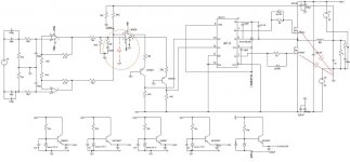
This is your scheme. the changes are only temporarily to eliminate the problems one at a time.
1) adjust pilot driver
2 we fix first input stage
3) adjust your loop FB
4) implements proper power Out
If you know that everything is OK, why do not you think it works?
I ... .. I create simulators and you use.🙂
1) adjust pilot driver
2 we fix first input stage
3) adjust your loop FB
4) implements proper power Out
If you know that everything is OK, why do not you think it works?
I ... .. I create simulators and you use.🙂
think carefully about the temporary change.
I unplugged the first stage (this is not in a ring of self-oscillating) but the influence of offset and gain of FB on input of comparator.
not you agree?
I unplugged the first stage (this is not in a ring of self-oscillating) but the influence of offset and gain of FB on input of comparator.
not you agree?
- Status
- Not open for further replies.
- Home
- Amplifiers
- Class D
- IR2110 failure with a scope probe